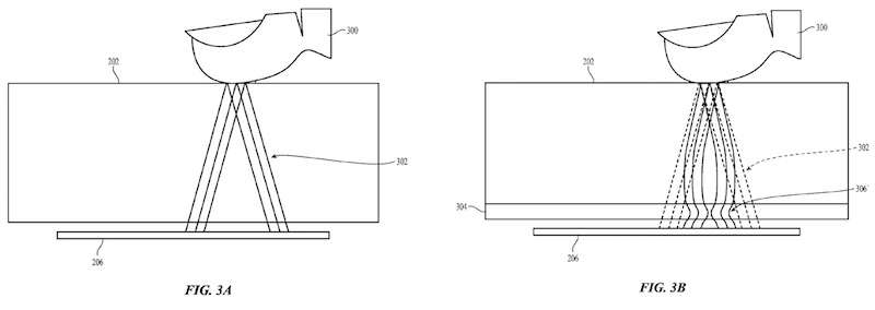
Credit: United States Patent, 9,460,332
(Tech Xplore)—"Capacitive fingerprint sensor including an electrostatic lens" is the title of the patent filed in September 2014.The inventor listed is Jean-Marie Bussat.
This is being talked about in this week's tech press as "Apple's electrostatic lens patent," which was first filed in September 2014. The patent description said, "This application generally relates to capacitive fingerprint sensing systems, and more particularly to the use of an electrostatic lens to increase the resolution of a capacitive sensing system."
Fundamentally, the news is about Apple patenting a fingerprint sensor "that works through displays," in the words of AppleInsider.
What's all this about "capacitive" sensors, and why is it important to Apple?
The patent said, "One example of a fingerprint recognition system uses capacitive sensing elements to detect fingerprint images for collection. Such sensors are able to detect electric field differences between ridges and valleys of the fingerprint of a finger in contact with a contact surface of the consumer electronic device adapted for this purpose."
However, there is a limitation which the patent description addresses, namely, space constraints.
The implementation of capacitive fingerprint sensors in devices with space constraints may lead to product designs with significant separation between the contact surface on which the user's finger is placed and the array of capacitive sensing elements. "The separation may lead to blurring of the electric field produced by the finger and reduced resolution of the capacitive fingerprint sensor."
Enter Apple's ideas for using electrostatic lenses. The use of electrostatic lenses may alleviate blurring caused by gaps.
The patent described the electrostatic lens concept as one or more patterned conductive layer(s).
"Each patterned conductive layer is located at a predetermined distance from the contact surface of the dielectric structure and is substantially parallel to the contact surface. These patterned conductive layers may be formed from various conductive materials, such as: copper; silver; aluminum; gold; nickel; titanium; tungsten; carbon nanotubes; polysilicon; indium tin oxide; conductive polymers or a combination thereof."
The patent said the conductive layers may be formed on dielectric layers within a dielectric structure, by processes such as deposition and etching or printing. The patterned conductive layers might be formed as separate elements, e.g., metal sheets fixed in place along the edges.
"During operation, each example patterned conductive layer may be substantially maintained at a predetermined voltage relative to the array of capacitive sensing elements."
Usually, tech watchers stress that companies' patent proposals may not turn up any time soon on the production lines. In this instance, though, there were suggestions that the patent concept may be applied in a future phone.
MacRumors' Mitchel Broussard: "As is usual with patents, it is unclear whether the electrostatic lens technology will show up in any future Apple device at all, much less one set to debut in less than a year, but its descriptive ability to fuel one of the iPhone 8's biggest rumors is interesting all the same."
Mikey Campbell of AppleInsider explained that in the case of common fingerprint sensors, separation between the contact surface where a user places their finger and the capacitive sensing array results in blurring of the finger's electric field, possible leading to degraded fingerprint image resolutions and decreased recognition accuracy.
Campbell said further that the patent overcomes design hurdles by introducing capacitive sensing technology that works through gaps in space, thereby allowing a future Touch ID module to sit behind iPhone's display."
More information: Capacitive fingerprint sensor including an electrostatic lens, United States Patent, 9,460,332.
© 2016 Tech Xplore


