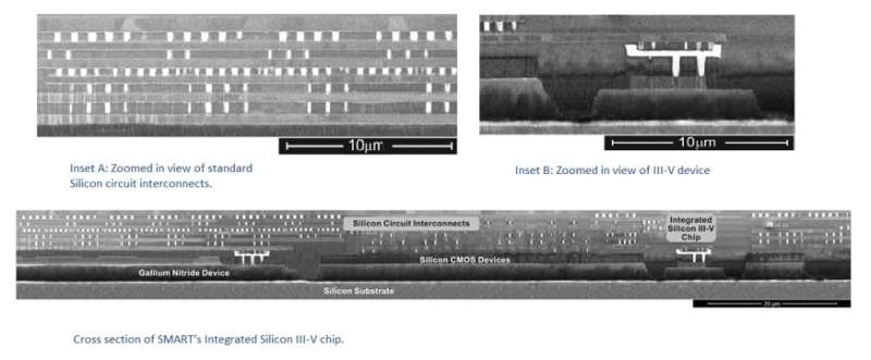
Cross section of SMART’s Integrated Silicon III-V chip. Credit: SMART
The Singapore-MIT Alliance for Research and Technology (SMART), MIT's Research Enterprise in Singapore, has announced the successful development of a commercially viable way to manufacture integrated Silicon III-V Chips with high-performance III-V devices inserted into their design.
In most devices today, silicon-based CMOS chips are used for computing, but they are not efficient for illumination and communications, resulting in low efficiency and heat generation. This is why current 5G mobile devices on the market get very hot upon use and would shut down after a short time.
This is where III-V semiconductors are valuable. III-V chips are made from elements in the 3rd and 5th columns of the elemental periodic table such as Gallium Nitride (GaN) and Indium Gallium Arsenide (InGaAs). Due to their unique properties, they are exceptionally well suited for optoelectronics (LEDs) and communications (5G etc) - boosting efficiency substantially.
"By integrating III-V into silicon, we can build upon existing manufacturing capabilities and low-cost volume production techniques of silicon and include the unique optical and electronic functionality of III-V technology," said Eugene Fitzgerald, CEO and Director, SMART, MIT's Research Enterprise in Singapore. "The new chips will be at the heart of future product innovation and power the next generation of communications devices, wearables and displays."
LEES researcher reviewing a 200 mm Silicon III-V wafer. The innovative and commercial-ready process by LEES leverages existing 200 mm semiconductor manufacturing infrastructure to create a new generation of chips that combines traditional Silicon with III-V devices, something not commercially viable before Credit: SMART
Kenneth Lee, Senior Scientific Director of the SMART LEES research program adds: "However, integrating III-V semiconductor devices with silicon in a commercially viable way is one of the most difficult challenges faced by the semiconductor industry, even though such integrated circuits have been desired for decades. Current methods are expensive and inefficient, which is delaying the availability of the chips the industry needs. With our new process, we can leverage existing capabilities to manufacture these new integrated Silicon III-V chips cost-effectively and accelerate the development and adoption of new technologies that will power economies."
The new technology developed by SMART builds two layers of silicon and III-V devices on separate substrates and integrates them vertically together within a micron, which is 1/50th the diameter of a human hair. The process can use existing 200mm manufacturing tools, which will allow semiconductor manufacturers in Singapore and around the world to make new use of their current equipment. Today, the cost of investing in a new manufacturing technology is in the range of tens of billions of dollars, thus this new integrated circuit platform is highly cost-effective and will result in much lower cost novel circuits and electronic systems.
SMART is focusing on creating new chips for pixelated illumination/display and 5G markets, which has a combined potential market of over $100B USD. Other markets that SMART's new integrated Silicon III-V chips will disrupt include wearable mini-displays, virtual reality applications, and other imaging technologies.
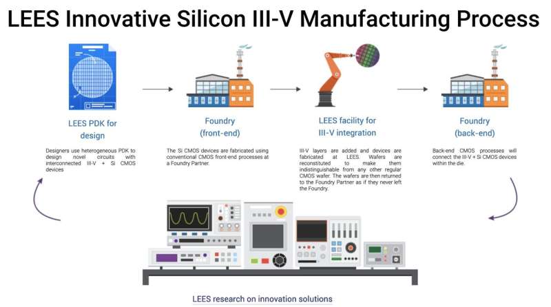
How LEES adds value to your production. Credit: SMART
The patent portfolio has been exclusively licensed by New Silicon Corporation Pte. Ltd. (NSC), a Singapore-based spin-off from SMART. NSC is the first fabless silicon integrated circuit company with proprietary materials, processes, devices, and design for monolithic integrated Silicon III-V circuits (www.new-silicon.com).
SMART's new integrated Silicon III-V chips will be available next year and expected in products by 2021.


