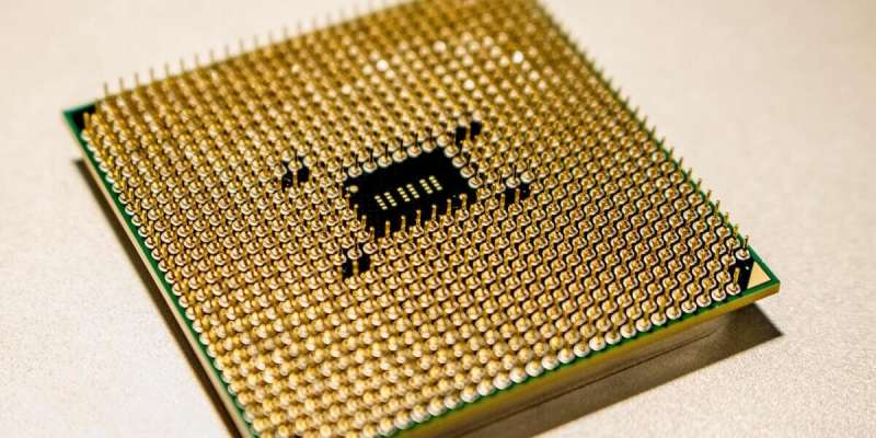
Credit: Jeremy Waterhouse, Pexels
From smartphones to laptops, in today's digital world, we rely on connectivity. One of the components underlying the smooth operation of these machines are silicon chips—semiconductors, which are an essential part of electronic circuits. They are also expensive.
As technology scaling continues, it enables smaller, faster and energy efficient electronics. Device dimensions are approaching the size of an atom, and with smaller prototypes, maintaining the same amount of production output as before has become challenging. The ultimate effect? Higher costs, which inevitably will get passed on to the consumer.
New strategies of defect identification and mitigation need to be developed to keep manufacturing of semiconductors efficient and keep devices, such as computers and smartphones more affordable. Assad Oberai, Hughes Professor in the USC Viterbi Department of Aerospace and Mechanical Engineering and interim vice dean of research for the school, and his colleagues have designed a deep learning algorithm that can identify defects in semiconductors, classify these defects and also map them as they occur.
"Imagine wiring a house. If there's one short circuit, then the whole system doesn't work. The same thing applies here," he said.
Instead of waiting for defects to occur and replicate across a batch, he suggests that this deep learning algorithm can be used to flag issues as they happen. In research published in the Journal of Micro/Nanolithography, Oberai, his graduate student Dhruv Patel, and Ravi Bonam, a semiconductor technology researcher at IBM Research, used a deep learning algorithm to identify defects when they occur. For example, imagine a solid line is being printed. If there is a break in that line, it would be considered incomplete or erroneous. The deep learning algorithm can identify when such a break occurs and also where exactly the break is located.
Patel, a USC Viterbi Ph.D. student in mechanical engineering, was also a part of the research team and won Honorable Mention for Best Student Paper at the SPIE Lithography Conference held in February 2019 for this work, co-authored with Oberai and Bonam.
How it works
With semiconductor manufacturing, just like in any other manufacturing process, anything can go wrong. "You can end up with something you didn't want, and in this case, those defects would mean that particular chip is useless and has to be thrown out," Oberai said.
"The tools that exist right now for doing this are very empirical or rules-based and therefore not very adaptable. If you print one circuit and then print a different circuit, you have to go back and tweak the rules manually to make sure it will work again," Oberai said. He also said that current tools pick up many false positives, meaning regions that aren't defective will be flagged and looked into. But alternately, if you're not conservative, you'll miss out on quite a few defects.
"The tradeoff between sensitivity and specificity is a difficult one. You don't want to end up with defects, but you also don't want to spend time and resources examining false positives," Oberai said.
In the research, accomplished in partnership with IBM, the team was able to achieve both high sensitivity (97%) and high specificity (100%), along with rapid and accurate defect localization.
Bonam said, "We are very encouraged by these results and this collaboration with academia indicates IBM Research's commitment to fundamentals to achieve deep expertise in A.I. technology."
The team achieved this by training the algorithm on a set of over 500 e-beam images (images created using electron technology that shows microscopic structural details)containing defects from three defect classes. Of these, about 40% had a single line breaks (defects covering a single line), 20% had multi-line breaks (defects span multiple lines) and 40% were defect-free.
Along the way, the team found that localization of the defect was a byproduct of the training. In other words, the same process that helped the algorithm identify and classify a defect allowed it to also discover where the defect was located.
Take an image and overlay it with a 20×20 grid, Oberai said. For each sub-region in this grid, you can ask the algorithm, was this region important in deciding whether or not there was a defect? "We repeated this question for every sub-region, and found that the region most important in making the decision on whether or not the semiconductor was defective was also the region that housed the line break," Oberai said.
Despite high accuracy in detecting defects, Oberai notes that the algorithm fails if it is trained for one type of pattern and applied to another. One work around, he said, is to infuse a small percentage of data from the new pattern to bring the algorithm along in being able to identify it. They found if they used 80% of the old pattern and 20% from the new pattern and mixed them up, accuracy improved significantly.
However, Oberai hopes to improve this process in the next phase of this research. "To me that is still unsatisfactory—the fact that you have to retrain it so significantly," Oberai said. Instead, he hopes they can create an algorithm that doesn't need to be trained in a supervised way at all. "Imagine a case where you give me thousands of images and say there is no defect in this image and give me nothing else. After that you give me images that may or may not have defects, then the algorithm will automatically flag images that have defects."
More information: Dhruv V. Patel et al. Deep learning-based detection, classification, and localization of defects in semiconductor processes, Journal of Micro/Nanolithography, MEMS, and MOEMS (2020). DOI: 10.1117/1.JMM.19.2.024801
Provided by University of Southern California


