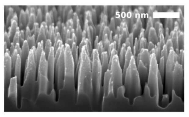
Bird’s eye view SEM image of b-Si nanotexture with columnar-like morphology. Credit: Physics Review Letters
"For the first time ever, we have direct experimental evidence that an external quantum efficiency above 100% is possible in a single photodiode without any external antireflection," says Hele Savin, associate professor of Micro and Nanoelectonics at Aalto University in Finland. The results come just a few years after Savin and colleagues at Aalto University demonstrated almost unity efficiency over the wavelength range 250-950 nm in photodiodes made with black silicon, where the silicon surface is nanostructured and coated to suppress losses.
Noticing some curious effects in the UV region, Savin's group extended their study of the devices to focus on this region of the electromagnetic spectrum. UV sensing has multiple applications, including spectroscopy and imaging, flame detection, water purification and biotechnology. While annual market demand for UV photodiodes is expected to increase to 30%, the efficiency of these devices has been limited to 80% at best. To Savin's surprise, closer analysis of their device's response to UV light revealed that the external quantum efficiency could exceed 130%. Independent measurements at Physikalisch Technische Bundesanstalt (PTB) verified the results.
Beating "theoretical limits"
In theory, if every photon that hit the photodiode knocked an electron or hole (charge carrier) into action, the efficiency would be 100%. However, several processes start to mop up these excited electrons or stop the photon from exciting them in the first place, leading to the oft-cited Schockley-Queisser theoretical limit for real devices of this kind.
Conversely, other effects can work in favour of higher efficiencies. It is now widely accepted that excited carriers can excite further carriers into action through collisions. Optimizing conditions for this "carrier multiplication" while staunching losses as much as possible would then seem a good bet for getting higher efficiency devices.
There are two main causes of loss: The first is photon reflection from the surface before it reaches the interior of the device to excite an electron, or hole, that will carry a current; the second is recombination of electron and hole pairs before they can make a meaningful contribution to the current. Here, Savin and her collaborators realised black silicon might really make a difference.
The surface of black silicon is nanostructured with cones and columns that make the surface highly absorbent at all angles that light might be incident. Usually, using nanostructured surfaces to lower reflection leads to greater recombination so little net gain is made, but these devices were coated in Al2O3 to suppress this recombination. The result was devices with not only near unity efficiency at wavelengths 250-950 nm, but efficiency exceeding 130% at 200 nm.
All you need is UV
Keen to determine what was enhancing the efficiency beyond 100%, the researchers simulated the electric field and electrostatic distribution in modeled nanocones and nanocolumns on a surface. "Our hypothesis was that it must be related to some quantum confinement or similar phenomenon as we were using nanometer-scale dimensions in our device," Savin says.
Surprisingly, the simulations showed no increase in electric field in the nanocones or nanocolumns, suggesting they were not responsible for enhancing the efficiency by boosting carrier multiplication or some other effect. Instead, the researchers found that once losses were suppressed, the high-energy UV photons could knock a carrier with enough clout to trigger a cascade of carrier multiplication, enhancing the device efficiency.
"In the past, the devices have suffered from optical and electrical losses, which have then masked the phenomenon that we are now seeing," explains Savin. "We were able to overcome the losses and fabricated a totally loss-free device, and therefore were able to go even beyond the theoretical limit of 100%." She also notes that since the material is silicon, it is also CMOS compatible, which is good news for industrial fabrication.
The simulations also revealed an odd disparity between the electric field, which was not higher in the middle of the nanostructures, and the electrostatic potential, which was. Usually, one follows the other, but Savin and collaborators explain the unusual difference in terms of the hole density needed to counter the fixed charge density of the Al2O3 coating. "The silicon nanostructures have changed from n-type to p-type (without using any dopant atoms)," says Savin. "So we are "virtually" doping the nanostructures."
The researchers are already in the process of commercializing their results through their spin-off company ElFys Inc., as well as trying to exceed 100% efficiency for other wavelengths, as well.
More information: M Garin et al, Black-silicon ultraviolet photodiodes achieve external quantum efficiency above 130%, Physics Review Letter (Just accepted) journals.aps.org/prl/accepted/ … 234ffbcb06f4a5ba1ac5 , arxiv.org/abs/1907.13397
© 2020 Science X Network


