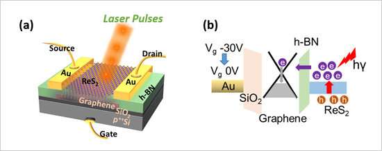
Figure 1. (a) Schematic diagram of the memory device structure composed of a stack of graphene, h-BN and ReS2 layers and the wired source and drain electrodes. (b) Band structure illustrating the charge accumulation process. Voltage and light are used in combination to control the amount of charge stored in the graphene layer. Credit: National Institute for Materials Science
The National Institute for Materials Science (NIMS) has developed a memory device capable of storing multiple values using both optical and voltage input values. This device composed of layered two-dimensional materials is able to optically control the amount of charge stored in these layers. This technology may be used to significantly increase the capacity of memory devices and applied to the development of various optoelectronic devices.
Memory devices used to store information (e.g., flash memory) play an indispensable role in today's information society. The recording density of these devices has substantially increased in the past 20 years. In anticipation of widespread adoption of IoT technologies in the near future, it is desirable to accelerate the development of higher speed, larger capacity memory devices. However, the current approach to increasing memory capacity and energy efficiency through silicon microfabrication is about to reach its limits. Development of memory devices with different working principles therefore has been awaited.
To meet expected technology needs, this research group has developed a transistor memory device composed of layered two-dimensional materials, including rhenium disulfide (ReS2)—a semiconductor—serving as a channel transistor, hexagonal boron nitride (h-BN) used as an insulating tunnel layer and graphene functioning as a floating gate. This device records data by storing charge carriers in the floating gate in a manner similar to conventional flash memory. Hole-electron pairs in the ReS2 layer are prone to excitation when irradiated with light. The number of these pairs can be regulated by changing the intensity of the light. The group succeeded in creating a mechanism that allows the amount of charge in the graphene layer to gradually decrease as the exited electrons once again couple with the holes in this layer. This success enabled the device to operate as a multivalued memory capable of efficiently controlling the amount of stored charge in stages through the combined use of light and voltage. Moreover, this device can operate energy efficiently by minimizing electric current leakage—an achievement made possible by layering two-dimensional materials, thereby smoothening the interfaces between them at an atomic level.
This technology may be used to significantly increase the capacity and energy efficiency of memory devices. It also may be applied to the development of various optoelectronic devices, including optical logic circuits and highly sensitive photosensors capable of controlling the amount of charge stored in them through combined use of light and voltage.
More information: Bablu Mukherjee et al. Laser‐Assisted Multilevel Non‐Volatile Memory Device Based on 2D van‐der‐Waals Few‐Layer‐ReS 2 /h‐BN/Graphene Heterostructures, Advanced Functional Materials (2020). DOI: 10.1002/adfm.202001688
Journal information: Advanced Functional Materials
Provided by National Institute for Materials Science


