Engineering team develops novel miniaturized organic semiconductor

Field Effect Transistors (FET) are the core building blocks of modern electronics such as integrated circuits, computer CPUs and display backplanes. Organic Field Effect Transistors (OFETs), which use organic semiconductor as a channel for current flows, have the advantage of being flexible when compared with their inorganic counterparts like silicon.
OFETs, given their high sensitivity, mechanical flexibility, biocompatibility, property tunability and low-cost fabrication, are considered to have great potential in new applications in wearable electronics, conformal health monitoring sensors, and bendable displays etc. Imagine TV screens that can be rolled up; or smart wearable electronic devices and clothing worn close to the body to collect vital body signals for instant biofeedback; or mini-robots made of harmless organic materials working inside the body for diseases diagnosis, target drug transportation, mini-surgeries and other medications and treatments.
Until now, the main limitation on enhanced performance and mass production of OFETs lies in the difficulty in miniaturizing them. Products currently using OFETs in the market are still in their primitive forms, in terms of product flexibility and durability.
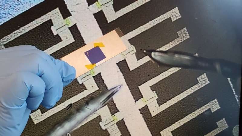
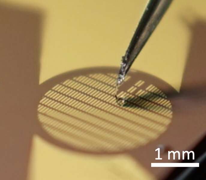
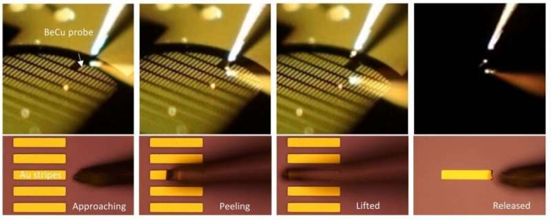
An engineering team led by Dr. Paddy Chan Kwok Leung at the Department of Mechanical Engineering of the University of Hong Kong (HKU) has made an important breakthrough in developing the staggered structure monolayer Organic Field Effect Transistors, which sets a major cornerstone to reduce the size of OFETs. The result has been published in the academic journal Advanced Materials. A US patent has been filed for the innovation.

The major problem now confronting scientists in reducing the size of OFETs is that the performance of the transistor will drop significantly with a reduction in size, partly due to the problem of contact resistance, i.e. resistance at interfaces which resists current flows. When the device gets smaller, its contact resistance will become a dominating factor in significantly downgrading the device's performance.
The staggered structure monolayer OFETs created by Dr. Chan's team demonstrate a record low normalized contact resistance of 40 Ω -cm. Compared with conventional devices with a contact resistance of 1000 Ω-cm, the new device can save 96% of power dissipation at contact when running the device at the same current level. More importantly, apart from energy saving, the excessive heat generated in the system, a common problem which causes semiconductors to fail, can be greatly reduced.
"On the basis of our achievement, we can further reduce the dimensions of OFETs and push them to a sub-micrometer scale, a level compatible with their inorganic counterparts, while can still function effectively to exhibit their unique organic properties. This is critical for meeting the requirement for commercialisation of related research." Dr. Chan said.
"If flexible OFET works, many traditional rigid based electronics such as display panels, computers and cell phones would transform to become flexible and foldable. These future devices would be much lighter in weight, and with low production cost."

"Moreover, given their organic nature, they are more likely to be biocompatible for advanced medical applications such as sensors in tracking brain activities or neural spike sensing, and in precision diagnosis of brain related illness such as epilepsy," Dr. Chan added.
Dr. Chan's team is currently working with researchers at the HKU Faculty of Medicine and biomedical engineering experts at CityU to integrate the miniaturized OFETs into a flexible circuit onto a polymer microprobe for neural spike detections in-vivo on a mouse brain under different external stimulations. They also plan to integrate the OFETs onto surgical tools such as catheter tube, and then put it inside animals' brains for direct brain activities sensing to locate abnormal activation in brain.
"Our OFETs provide a much better signal-to-noise ratio. Therefore, we expect we can pick up some weak signals which cannot be detected before using the conventional bare electrode for sensing."
"It has been our goal to connect applied research with fundamental science. Our research achievement would hopefully open a blue ocean for OFETs research and applications. We believe that the setting and achievement on OFETs are now ready for applications in large area display backplane and surgical tools." Dr. Chan concluded.
More information: Boyu Peng et al. Crystallized Monolayer Semiconductor for Ohmic Contact Resistance, High Intrinsic Gain, and High Current Density, Advanced Materials (2020). DOI: 10.1002/adma.202002281


