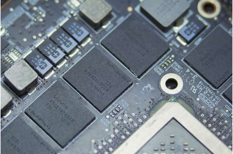
Study of indium arsenide paves way to smaller, more powerful electronics

Skoltech researchers have studied the electronic properties of indium arsenide, a semiconductor that is currently widely used for photodiodes in the infrared range and proposed as a building block for alternative infrared lasers and terahertz oscillators. The paper was published in the journal Physical Chemistry Chemical Physics.
As electronic devices keep getting smaller while their performance increases, engineers are increasingly looking at so-called III–V compound semiconductors. These materials, featuring high electron transport properties in comparison to conventional silicon, provide an alternative path to overcome current key technological bottlenecks such as electronic device performance along with its miniaturization. One of them is indium arsenide (InAs), which has exceptionally high electron mobility and carrier density, meaning that it can process the signal faster at low supply voltage and consequently increase the computation efficiency of a device.
"The study of material properties requires a detailed understanding of its surface structure that might exhibit a large variety of reconstructions—ordering at the surface—depending on the manufacturing process, sample orientation, and external effects," Anastasia Pervishko, research scientist at the Skoltech Center for Computational and Data-Intensive Science and Engineering (CDISE) and a co-author of the paper, says.
Pervishko and her Skoltech colleagues, Ivan Vrubel and Dmitry Yudin, conducted a comprehensive theoretical analysis of the electronic structure of InAs(111) surfaces. They were able to show that their evaluations for some of the compound parameters as well as surface reconstructions were consistent with previously reported experimental results.
"An interesting feature of InAs surfaces is natural electron accumulation in the near-surface area that allows one to utilize it as a platform for novel low-dimensional quantum systems. We found stable surface configurations and, in view of available experimental insights, were able to distinguish the origin of accumulation layer formation depending on material orientation," Pervishko says.
Surface effects start playing a key role as devices get smaller, so a detailed understanding of material surface structure and charge distribution is necessary for subsequent potential applications, she adds.
"For now, we limited our consideration to the study of a clean InAs surface. Following current scientific trends, we need to understand the effects related to the atomic layer deposition on InAs surfaces," Pervishko concludes.
More information: Ivan I. Vrubel et al, On the origin of the electron accumulation layer at clean InAs(111) surfaces, Physical Chemistry Chemical Physics (2021). DOI: 10.1039/D0CP05632D


