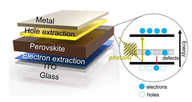
A schematic of a perovskite solar cell, showing that the perovskite is nestled in the center of the cell. Absorption of solar light causes the electrons to jump to higher energy levels, leaving the holes behind. Further separation of the electrons and the holes results in the generation of a current. The existence of defects that might trap the electrons or the holes, can cause the whole solar cell to lose efficiency. Credit: Okinawa Institute of Science and Technology
The expansion of solar energy is a necessity to sustainably meet the world's energy demands. To achieve this, researchers have focused on the development of semiconducting energy materials. One such material, hybrid perovskites, consists of both organic and inorganic ions. These are promising candidates to form the next generation of solar cells, which could be more cost effective and more easily mass produced than the conventional ones currently available.
But, before they can be commercialized, their efficiency needs to be expanded and their limits properly understood. Writing in Energy & Environmental Science, researchers from the Femtosecond Spectroscopy Unit, led by Professor Keshav Dani, at the Okinawa Institute of Science and Technology Graduate University (OIST) and Optoelectronics Materials and Device Spectroscopy Group, led by Dr. Sam Stranks at the University of Cambridge identified three different kinds of defect clusters in state-of-the-art perovskite thin films, which likely form during the perovskite's fabrication and may impede efficiency.
"If you have a solar cell, you want the whole material to contribute to converting sunlight to electricity, otherwise you are not utilizing its full potential, which is not desirable for commercial purposes," said Sofiia Kosar, Ph.D. candidate in the OIST Unit and first author of the research paper.
The perovskite material lies at the heart of the solar cell, which consists of many different layers. When the sun hits the solar cell, its energy is absorbed by the perovskite, causing electrons to jump into a higher energy level and leaving holes behind. All the electrons then move in one direction through the layers of the solar cell to the electrical contact and the holes, in the other direction, thus generating a current.
"If there are defects within the material this might impact the generation of electron-hole pairs or their collection at contacts and mean that the perovskite solar cell loses efficiency," Sofiia said. She went on to explain that theoretically, perovskite solar cells could convert about 30% of incident light to electricity. "Right now, hybrid perovskites regularly output between 20% and about 25%."
Experts in the field were aware of the existence of defects that might impede efficiency, but it was previously unclear whether these defects all had the same characteristics and could thus be removed using one strategy. In this study, by using state-of-the-art equipment, the defects were imaged and characterized with a nanoscale resolution to reveal three distinct kinds.
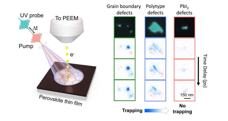
The researchers conducted a time-resolved photoemission experiment to understand the role of each defect in perovskite performance. As can be seen in the graph on the right, the grain boundary defects, despite their small size, were the most detrimental for charge carrier trapping, which results in undesirable performance losses for the solar cell. Credit: Okinawa Institute of Science and Technology
The most detrimental kind the researchers found was the grain boundary defect. These defects are tiny and, as the name suggests, sit at the boundary between different crystal grains of perovskite. They seemed to actively trap photogenerated holes and deplete efficiency from the regions far exceeding their size, thus causing huge issues for the performance of the perovskite.
Then there are polytype defects. These occur when the precursor material crystallizes, not in the typical cubic perovskite structure, but a hexagonal one. This type of defect cluster is relatively big and also negatively impacts efficiency by trapping photogenerated holes.
"If there are a lot of polytype defects in a film, their impact can become just as detrimental as the grain boundary ones," Sofiia explained. "Both the grain boundary and the polytype defects need to be targeted by developing specific strategies."
Finally, the study revealed the lead iodide defects. These form from precipitated lead iodide—an important part of perovskite material that is used during the fabrication. However, this research suggests that they seem to be benign in terms of trapping charges from perovskite and have little impact on efficiency.
The researchers decided to use an approach that is often used to reduce defect density in perovskites—treatment with light and oxygen—to see how these defects would respond. They did this by exposing the perovskite to visible light and a mildly oxygenated atmosphere. Interestingly, they found that the defects reacted in different ways. For example, the most detrimental grain boundary defects were healed and stopped trapping the holes. However, the effect on the other defect types was more nuanced and not necessarily beneficial.
"This research shows that we likely need targeted approaches to address the undesired effects of the different defect types, and thus improve the performance of perovskite solar cells," concluded Prof. Dani.
More information: Sofiia Kosar et al, Unraveling the varied nature and roles of defects in hybrid halide perovskites with time-resolved photoemission electron microscopy, Energy & Environmental Science (2021). DOI: 10.1039/d1ee02055b
Journal information: Energy & Environmental Science
Provided by Okinawa Institute of Science and Technology


