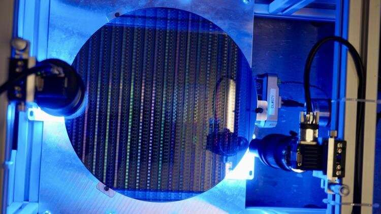
The device uses two cameras to capture the wafer's edge. Credit: University of Colorado at Boulder
The shortage of semiconductors—the computer chips that products such as smartphones, laptops, cars and even washing machines rely on—continues to impact industries around the world.
The current supply chain issues are motivating engineers to make the inspection of the silicon wafers that semiconductors are fabricated from more efficient. It is a goal that the industry would focus on even without the global shortage. To help accomplish that, University of Colorado mechanical engineering students have developed a device that improves the inspection process.
The Department of Mechanical Engineering seniors have built a silicon wafer center-finding improvement device for KLA, a semiconductor manufacturing company. The Senior Design team's prototype uses two cameras to capture the circular wafer's edge, plus computer software to calculate the radius and find the wafer's center.
"The reason this is important is that KLA has to inspect these wafers for defects, and when they find one, they need to know where on the wafer it is with a high-level of precision," said Marty LaRocque, the team's electro-mechanical engineer. "They have to establish a coordinate system on the wafer and the hardest part of that is finding the center."
Currently, KLA is detecting the wafer's center with ten different images around the edge. The team of students designed their device to find the center just as efficiently with only two images.
"On one of KLA's inspection tools, it currently takes them eight seconds to align one wafer, and we're trying to get that down to two seconds," said Project Manager Jack Carver. "A 75% reduction is going to get so much more throughput. With the global silicon wafer supply shortage, any improvements in that would be greatly beneficial for them."
The real-world impact that the students' device could have on the industry is part of the reason this project enticed them.
"It's interesting because KLA explained to us the real significance of our prototype," said Prem Griddalur, the systems engineer on the team. "About every two years, the size of the semiconductor becomes smaller, and at the same time, the scale they're manufacturing these at gets larger because of increased demand. KLA did a great job explaining why their equipment is important and how our project plays a role in the larger scheme of the industry."
The team captured their first position of the wafer's center in early March. They are now running statistical tests and taking measurements to check the device's accuracy. They need the coordinates to be within 10 microns of the true center, which is the width of a human red blood cell.
Since the team's device is a prototype, KLA's system may not end up looking exactly like the students' design. However, their prototype and tests will still provide the company with critical information to help guide decisions about future designs.
The students said that aspect is relatable to real-world scenarios. Typically, engineers are tasked with making current systems better, rather than creating new designs from scratch.
"That's what our prototype is—improving upon KLA's system," said CAD Engineer Hank Kussin-Bordo. "We were given the requirement that our design has to work with the company's current system, since they can't change their entire process. The challenge of being an engineer is finding ways to make systems better, while also being cost effective and not over-complicating things."
Designing, assembling and testing the device have also allowed the students to work at the intersection of engineering and electronics—a collaboration that the team agreed is the future of modern engineering.
"When the images from our two cameras show the tiny little patterns that are printed on the wafer that you can't see with the naked eye, we all feel a sense of wow, that's some real-life engineering right there," said Carver.
The Senior Design team will present their silicon wafer center-finding improvement device at the College of Engineering and Applied Science Engineering Projects Expo 2022 on April 22.
More information: Expo: www.colorado.edu/engineering/expo
Provided by University of Colorado at Boulder


