This article has been reviewed according to Science X's editorial process and policies. Editors have highlighted the following attributes while ensuring the content's credibility:
fact-checked
proofread
Dark current modeling of thick perovskite X-ray detectors

X-ray detection is widely used in medical imaging, radioactivity detection, security checking, industrial flaw inspection, and so on. In recent years, metal halide perovskites have demonstrated excellent performances in the detection of X-rays and gamma-rays. However, most studies focus on perovskite single-pixel devices. To achieve the application goal of X-ray imagers, the detectors should be integrated with pixel circuits.
This means that the device dark current is an important figure of merit to be considered. The low dark current can guarantee the response range and reduce noise fluctuations. In general, constructing junction devices is effective in suppressing the dark current. But for thick perovskite X-ray detectors, the performances of junction devices are generally poor, especially for p–n junctions. The underlying mechanism is still not clear.
A team of researchers, led by Prof. Guangda Niu from Wuhan National Laboratory for Optoelectronics, Huazhong University of Science and Technology, China, summarized and built a dark current model for thick perovskite X-ray detectors.
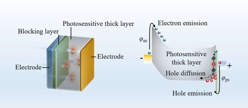
They quantitatively evaluated the dark current requirement for X-ray imagers integrated with pixel circuits, which is as low as nanoampere per square centimeter. Moreover, as revealed by the semiconductor device analysis and simulation, the main current components of thick perovskite X-ray detectors include two kinds, the thermionic-emission current and the generation-recombination current.
They designed multiple groups of experiments on Schottky and p-n junction device structures, to show that the typically observed failures of p–n junctions in thick detectors are caused by the high generation-recombination current due to the hetero-band mismatch and interface defects. The researchers believe that this work can provide a deep insight into the design of high sensitivity and low dark current perovskite detectors applying to X-ray imagers.
The work was published on Frontiers of Optoelectronics.
More information: Shan Zhao et al, Dark current modeling of thick perovskite X-ray detectors, Frontiers of Optoelectronics (2022). DOI: 10.1007/s12200-022-00044-1


