Credit: Fukamachi et al
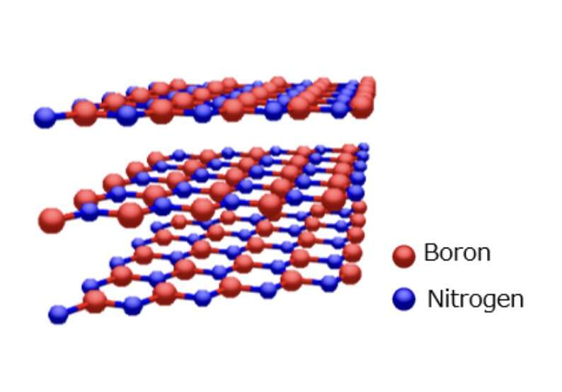
Researchers at Kyushu University, the National Institute of Advanced Industrial Science and Technology (AIST) and Osaka University in Japan have recently introduced a new strategy for synthesizing multi-layer hexagonal boron nitride (hBN), a material that could be used to integrate different 2D materials in electronic devices, while preserving their unique properties. Their proposed approach, outlined in a paper published in Nature Electronics, could facilitate the fabrication of new highly performing graphene-based devices.
"The atomically flat 2D insulator hBN is a key material for the integration of 2D materials into electronic devices," Hiroki Ago, one of the researchers who carried out the study, told Tech Xplore. "For example, the highest carrier mobility in monolayer graphene is achieved only when it is sandwiched by multilayer hBN. Superconductivity observed in twisted bilayer graphene also needs multilayer hBN to isolate from environment."
In addition to its value for fabricating graphene-based devices, hBN can also be used to integrate transition metal dichalcogenides (TMDs) in devices, achieving strong photoluminescence and high carrier mobility. It can also be valuable for conducting studies focusing on moiré physics.
Despite its many possible uses, so far the synthesis of high-quality hBN has proved to be challenging, particularly compared to the synthesis of other 2D materials. The hBN produced using existing methods are generally too thin or not homogenous.
"Although promising results have been achieved using chemical vapor deposition (CVD), it is only limited to monolayer hBN, but monolayer hBN is not thick enough to screen out the environmental effects," Ago said. "Thus, controlling the thickness of hBN is still challenging due to complex interactions between the B and N species and the catalytic substrate."
Credit: Fukamachi et al
The key objective of the recent study by Ago and his colleagues was to identify a strategy for producing hBN with a uniform thickness at different scales that meet the needs of different devices. The team also wished to enable the successful integration of the synthesized hBN with graphene, achieving reliable and highly performing devices at a wafer-scale.
The strategy they devised is based on CVD, a chemical process commonly used to grow hBN and other 2D materials. While this process was applied in previous works, it did not always result in homogenous and good quality hBN.
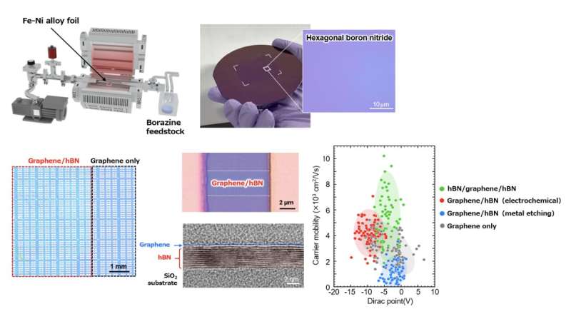
"The process involves exposing a metal substrate (polycrystalline Fe-Ni foil in our case) to a gas containing the precursors of the hBN (B and N), which undergo chemical reactions at high temperatures to create layers of hBN on the surface of the Fe-Ni," Ago explained. "By tuning the relative amount of Fe and Ni, a uniform segregation of hBN can be obtained. In addition to the CVD growth, transfer from the metal catalyst is also very important, because it strongly influences the physical properties."
To transfer the hBN they had grown onto graphene, Ago and his colleagues used a material transfer technique known as electrochemical delamination, leveraging the H2 bubbles formed at the interface of the Fe-Ni and the hBN layers. While this process is known to be cleaner and more efficient than other material transfer methods, they found that the interface between the hBN and graphene layer was not as clean as they would have liked and would thus not produce uniform graphene devices at a wafer scale.
"To address this issue, we systematically studied the effects of various cleaning and treatment processes on the transferred hBN and on subsequent graphene," Ago said. "We found that sequential annealing in a H2 environment at high temperatures ensures relatively clean interfaces between the hBN and the graphene."
Credit: Fukamachi et al
Using their proposed hBN synthesis and transfer approach, the researchers were able to fabricate highly performing devices where graphene was encapsulated by hBN. These devices were found to outperform other devices in which graphene was placed directly on an SiO2 layer.
"This performance improvement, which has previously been observed for devices carefully patterned at specific clean and homogeneous locations, was observed here for the first time for devices produced at wafer-scale using procedures compatible with mass-production techniques," Ago said. "We demonstrated the successful synthesis of high quality hBN at large scales using relatively inexpensive Fe-Ni foils and developed scalable transfer processes that enabled the fabrication of graphene devices with improved performance at wafer-scale."
This recent study by Ago and his colleagues demonstrates the potential of CVD-grown 2D materials for the mass-production of highly performing and uniform electronics. In the future, the strategy they developed could be used to reliably produce uniform hBN on a large-scale and then integrate it in different devices.
Ago and his colleagues now plan to improve their synthesis and transfer processes further, to facilitate their introduction in both research and industry settings. For instance, the hBN produced during their experiments shows a homogeneous thickness ranging between 5–10 nm across a wafer, which might be not meet the requirements of particularly complex and demanding electronic applications.
"The ability to produce thicker hBN films would redound in better isolation of other 2D materials, but it has been proven to be challenging to increase the thickness while maintaining the uniformity," Ago added. "We are thus now working to improve our synthesis methods. Additionally, our current transfer process relies on using a PMMA sacrificial layer, so we are currently investigating alternative methods that result in cleaner transferred hBN and that are more amenable to industrial-scale processing, allowing to increase the processing throughput while maintaining the device quality."
More information: Satoru Fukamachi et al, Large-area synthesis and transfer of multilayer hexagonal boron nitride for enhanced graphene device arrays, Nature Electronics (2023). DOI: 10.1038/s41928-022-00911-x
Journal information: Nature Electronics
© 2023 Science X Network


