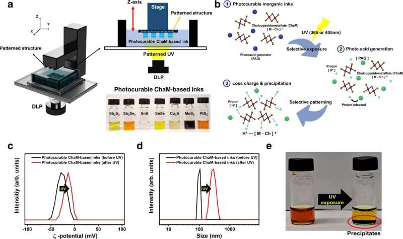
Generalized optical printing of metal chalcogenide. a Schematic of the digital light processing (DLP)-based optical printing of chalcogenidometallate (ChaM)-based inks. The DLP process that operates by reflecting light off digital micro-mirror devices selectively solidifies the photocurable metal chalcogenide inks and create complex 2D films and 2.5D architectures by 2D layer-by-layer curing. b Photocuring mechanism of the photocurable ChaM-based inks. The ChaMs react with the protons generated by the photoreaction of the photoacid generators (PAGs), causing precipitation of the ChaMs. c ξ-potential (zeta potential), d Dynamic light scattering (DLS) size, and e photograph of the photocurable ChaM-based inks before (black line) and after (red line) ultraviolet (UV) irradiation. Credit: Nature Communications (2022). DOI: 10.1038/s41467-022-33040-2
Patterning of materials is considered an essential prerequisite for the fabrication of high-resolution and high-performance devices. Various methods have been developed, yet conventional manufacturing processes often require multi-step processes or expensive lithography equipment.
A research team, affiliated with UNIST has recently unveiled a new patterning technique, which is as simple as the photo printing process. This breakthrough has been jointly led by Professor Jae Sung Son (Department of Materials Science and Engineering) and Professor Jiseok Lee (School of Energy and Chemical Engineering) from UNIST.
In this study, the research team reported a generalized direct optical printing technique to obtain functional metal chalcogenides via digital light processing (DLP). In doing so, the research team developed universally applicable photocurable chalcogenidometallate (ChaM)-based inks that could be directly used to create 2D patterns or micrometer-thick 2.5D architectures of various sizes and shapes.
According to the research team, their process is applicable to a diverse range of functional metal chalcogenides for compound semiconductors and 2D transition-metal dichalcogenides. The research team also demonstrated the feasibility of our technique by fabricating and evaluating a micro-scale thermoelectric generator bearing tens of patterned semiconductors.
"We believe that our technology, in combination with high-resolution equipment, such as two-photon lithography, can realize the patterning of inorganic materials with excellent quality and resolution," noted the research team
"Our DLP-based optical printing technology presents an alternative approach to photolithography and can serve as a platform technology for the cost-effective, simple, and high-resolution direct architecturing of inorganic materials."
Their findings have been published in Nature Communications.
More information: Seongheon Baek et al, Generalised optical printing of photocurable metal chalcogenides, Nature Communications (2022). DOI: 10.1038/s41467-022-33040-2
Journal information: Nature Communications


