The world's smallest high-performance magnetic tunnel junction

A research group from Tohoku University led by current president Hideo Ohno has developed the world's smallest (2.3 nm) high-performance magnetic tunnel junctions (MTJs). This work is expected to accelerate the advancement of ultrahigh-density, low-power, high-performance non-volatile memory for a variety of applications, such as IoT, AI, and automobiles.
The development of STT-MRAM—non-volatile spintronics memory—helps reduce the increasing power consumption in semiconductor device scaling. Crucial to integrating STT-MRAM in advanced integrated circuits is scaling magnetic tunnel junction—a core component of STT-MRAM—while improving its performance in data retention and write operation.
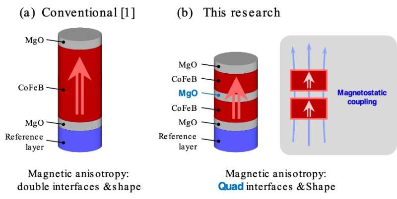
Shape-anisotropy MTJ, proposed by the same group in 2018, has shown MTJ scaling down to single-digit nanometers while achieving sufficient data-retention (thermal-stability) properties. In the shape-anisotropy MTJ, thermal stability is enhanced by making the ferromagnetic layer thick. Once the thickness goes beyond a certain point, however, device reliability becomes degraded.
To address the issue in the conventional shape-anisotropy MTJ with a single ferromagnetic structure [Fig. 1(a)], the group employed a new structure that uses magnetostatically coupled multilayered ferromagnets [Fig. 1(b)]. The developed MTJs were successfully scaled down to 2.3 nm in diameter—the world's smallest MTJ size. They also exhibited high data retention properties up to 200°C and high-speed and low-voltage write operation down to 10 ns below 1 V at a single-digit-nanometer scale.
"The performance proves the developed MTJs' capability to work with the future-generation advanced integrated circuits," said Butsurin Jinnai, first author of the study. "Because of its material compatibility with the standard MTJ material system, CoFeB/MgO, the proposed MTJ structure can be easily adopted in existing MTJ technology." The group believes that this will speed up the development of ultrahigh-density, low-power, high-performance memory for a variety of applications, such as IoT, AI, and automobiles.
More information: High-Performance Shape-Anisotropy Magnetic Tunnel Junctions down to 2.3 nm, Butsurin Jinnai*, Junta Igarashi*, Kyota Watanabe, Takuya Funatsu, Hideo Sato, Shunsuke Fukami, and Hideo Ohno. Conference: IEEE International Electron Devices Meeting (IEDM)


