January 12, 2023 feature
This article has been reviewed according to Science X's editorial process and policies. Editors have highlighted the following attributes while ensuring the content's credibility:
fact-checked
peer-reviewed publication
trusted source
proofread
A method to reliably fabricate transition metal dichalcogenide field-effect transistors on a wafer-scale

Electronics engineers are continuously trying to develop thinner, more efficient and better performing transistors, the semiconductor devices at the core of most modern electronics. To do this, they have been evaluating the potential of a broad range of materials.
Transition metal dichalcogenides (TMDs), compounds based on transition metals and chalcogen elements, have very attractive electronic and mechanical properties that make them promising candidates for the development of future generations of transistors. Most notably, they have an atomically thin structure with no dangling bonds and a bandgap similar to that of silicon.
Despite their advantageous characteristics, TMDs have not yet been used to create transistors on a large scale. The main reason for this is the weak adhesion energy at the interface between these materials and substrates, which makes their widespread fabrication challenging.
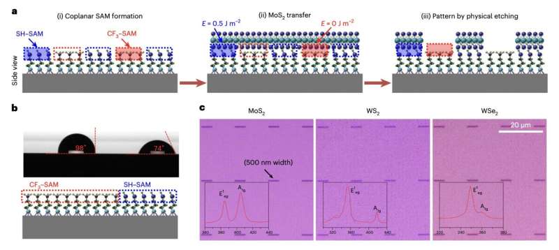
Researchers at Samsung Electronics and University of Chicago have recently identified a strategy that could enable the reliable integration of TMD-based field-effect transistors (FETs) on a wafer scale. Their proposed approach, introduced in a paper published in Nature Electronics, is based on the use of adhesion lithography, an innovative technique to form nanoscale gaps between samples of dissimilar materials.
"Field-effect transistors based on two-dimensional materials are a potential replacement for silicon-based devices in next-generation semiconductor chips," Van Luan Nguyen and his colleagues wrote in their paper. "However, the weak interfacial adhesion energy between two-dimensional materials and substrates can lead to low yields and non-uniform transistors on the wafer scale. Furthermore, conventional photolithography processes—including photochemical reactions and chemical etching—can damage atomically thin materials."
As part of their study, Nguyen and his colleagues demonstrated that the interfacial adhesion energy (IAE) between 2D materials and different substrates can be quantified using a four-point bending method. They then grew 2D materials molybdenum disulfide (MoS2) and graphene using chemical vapor deposition.
Subsequently, they studied the effect of intrinsic material defects on the materials' IAE value over a large surface area. To form interfaces between the materials and substrates, they ultimately transferred the materials onto a metal or insulating layer.
"We show that the interfacial adhesion energy between two-dimensional materials and different substrates can be quantified using a four-point bending method," Nguyen and his colleagues explained in their paper. "We find that a molybdenum disulfide/silicon dioxide interface has an interfacial adhesion energy of 0.2 J m−2, which can be modulated from 0 to 1.0 J m−2 by incorporating self-assembled monolayers with different end-termination chemistries. We use this to create an adhesion lithography method that is based on adhesion energy differences and physical etching processes."
Nguyen and his colleagues demonstrated the feasibility of their fabrication strategy by using it to produce over 10,000 molybdenum disulfide FETs based on six-inch wafers, attaining an impressive yield of almost 100%. In the future, their proposed method could be perfected and improved further, potentially enabling the large-scale fabrication of FETs based on TMDs, by reducing errors and improving the adhesion between these materials and substrates.
More information: Van Luan Nguyen et al, Wafer-scale integration of transition metal dichalcogenide field-effect transistors using adhesion lithography, Nature Electronics (2022). DOI: 10.1038/s41928-022-00890-z
© 2023 Science X Network


