This article has been reviewed according to Science X's editorial process and policies. Editors have highlighted the following attributes while ensuring the content's credibility:
fact-checked
trusted source
proofread
Innovative extreme ultraviolet lithography technology dramatically benefits of semiconductor manufacturing

Professor Tsumoru Shintake of Okinawa Institute of Science and Technology (OIST) has proposed an extreme ultraviolet (EUV) lithography technology that surpasses the standard in semiconductor manufacturing.
EUV lithography based on this design can work with smaller EUV light sources, reducing costs and dramatically improving reliability and lifetime of the machines. It also consumes less than one-tenth the power of conventional EUV lithography machines, helping the semiconductor industry become more environmentally sustainable.
This technology has been made possible by solving two issues that were previously considered insurmountable in this field. The first involves a novel optical projection system consisting of only two mirrors. The second involves a new method to efficiently direct EUV light onto logic patterns on a flat mirror (the photomask) without blocking the optical path.
Challenges surrounding EUV lithography
The processors making artificial intelligence (AI) possible, low-power chips used in mobile devices like cell phones, and high-density DRAM memory used in machines that have become indispensable in our daily lives—all these advanced semiconductor chips are manufactured using EUV lithography. However, the production of semiconductors is challenged by the high-power consumption and complexity of the equipment, which dramatically increases the cost of installation, maintenance, and in power consumption.
As Prof. Shintake puts it, "This invention is a breakthrough technology that can almost completely solve these little-known problems."
In traditional optics systems, such as cameras, telescopes and conventional ultraviolet lithography, optical components like the aperture and lenses are arranged axisymmetrically (symmetric to the central axis) in a straight line. This configuration ensures the highest optical performance, with minimal optical aberrations, achieving high quality images. However, this does not work for EUV rays, as they have extremely short wavelengths that are absorbed by most materials, meaning that they cannot travel through transparent lenses.
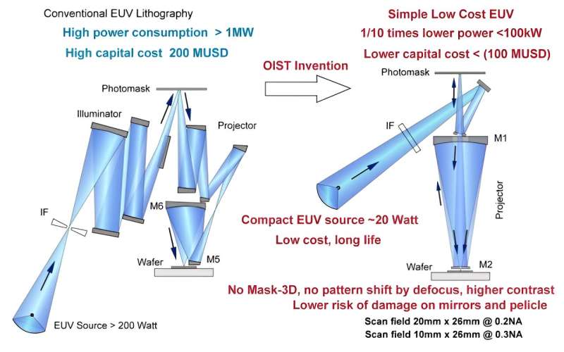
For this reason, EUV light is directed using crescent-shaped mirrors that reflect the rays along the optical path in a zigzag pattern through open space (see the illustration below). However, because this method causes light to deviate from the central axis, it sacrifices important optical properties and reduces the overall performance of the system.
To combat this issue, this new lithography technology achieves its superior optical properties by aligning two axisymmetric mirrors with tiny center-holes in a straight line.
Significant reduction in power consumption
EUV energy weakens by 40% with each mirror reflection because of its very high absorbency. In the industry standard, only about 1% of the energy from the EUV light source reaches the wafer through the 10 mirrors used, which means that a very high EUV light output is required. To meet this demand, the CO2 laser drive for the EUV light source requires a large amount of electric power, as well as a huge amount of water for cooling.
In contrast, by limiting the number of mirrors to just four in total from EUV source to wafer, more than 10% of the energy makes it through, meaning that even a small EUV source with an output of a few tens of watts can work just as effectively. This can lead to significant reduction in power usage.
Two challenges overcome
The projector at the heart of EUV lithography, which transfers the photomask image onto the silicon wafer, consists of only two reflective mirrors, like an astronomical telescope.
"This configuration is unimaginably simple, given that conventional projectors require at least six reflective mirrors. This was made possible by carefully rethinking the aberration correction theory of optics. It is a triumph of classical physics before quantum physics," explains Prof. Shintake.
"The performance has been verified using optical simulation software (OpTaliX) and it is guaranteed to be sufficient for the production of advanced semiconductors."
Professor Shintake solved the problem by devising a new method of illumination optics, named the "dual line field," which irradiates a flat mirror photomask with EUV light from the front without interfering with the optical path.
Professor Shintake explains, "If you hold two flashlights, one in each hand, and aim them diagonally at a mirror in front of you at the same angle, then the light from one flashlight will always hit the opposite flashlight, which is unacceptable in lithography. But if you move your hands outward without changing the angle of the flashlights until the middle is perfectly lit up from both sides, the light can be reflected without colliding with the light from the opposite flashlights."
Since the two light sources are symmetrically positioned and illuminate the mask at the same angle, on average the mask is illuminated from the front. This also minimizes mask 3D effects.
"It's like the egg of Columbus," explains Prof. Shintake, "in that it may seem impossible at first glance, but once solved, it becomes very simple."
OIST has filed a s patent application for this technology, and it is expected to be put to practical use through demonstration experiments. "The global EUV lithography market is expected to grow from 8.9 billion USD in 2024 to 17.4 billion USD in 2030, with an average annual growth rate of approximately 12%. This patent has the potential to generate tremendous economic benefits," summarizes Prof. Shintake.
Gil Granot-Mayer, OIST Executive Vice President and leader of OIST Innovation, says, "OIST is committed to creating cutting-edge science that will impact humanity. This innovation captures the OIST spirit of exploring the impossible and offering original solutions.
"lthough we still have a long way to go in developing this technology, we are committed to doing so. We hope that this technology from Okinawa will have a transformative impact on the semiconductor industry and help solve global issues such as energy consumption and decarbonization."


