July 23, 2017 weblog
ASML lithography team turns corner in throughput spec of wafers per hour
(Tech Xplore)—Last year, lithography held a major share of the semiconductor manufacturing equipment market than other equipment (WhaTech). "Lithography has progressed over the past few years because of extensive R&D in this field."
Netherlands-based ASML are a dominant supplier of lithography equipment for semiconductor wafer manufacturing. "As a company that makes the lithography machines to manufacture these chips, Moore's Law also drives our business. In fact, the key to making transistors on a chip smaller is lithography."
The company stated that lithography is "arguably the most important and critical part of the chip production process." It determines how much circuitry can be packed onto a chip, they said, controlling the size and shape of all chip components, connections and contacts.
They noted it is used in making every layer of the chip, about 30 steps, they said, to selectively grow, modify and etch out the features.
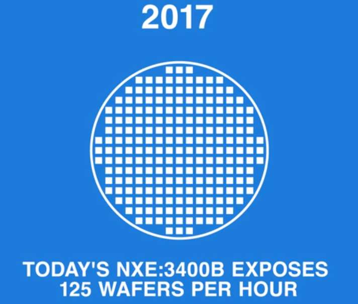
Now ASML tests achieved the throughput specification of 125 wafers per hour. Throughput was the final key spec that needed to be demonstrated and the numbers are of interest to industry watchers.
Mark Tyson in HEXUS:
"ASML has successfully demonstrated a 250-watt EUV source which will accelerate wafer throughput up to about 125 wafers per hour (WPH). Industry watchers had seen the inability of ASML to reach this throughput figure as a major roadblock in EUV development."
Dylan McGrath in EE Times: "The demonstration of 125 WPH productivity is considered a key milestone for EUV tools. Chip vendors have long insisted that EUV tools must be capable of this level of throughput to be cost effective in volume manufacturing."
"In EUV lithography, we have integrated an upgraded EUV source into a TWINSCAN NXE:3400B lithography system in our Veldhoven facility and achieved the throughput specification of 125 wafers per hour on this system," according to the ASML press release.
"In just over ten years, we took EUV lithography from hours per wafer to wafers per hour."
How EUV plays its role:
"System wafer throughput is dependent on several parameters including the amount of power the EUV light source can generate. This is because an exposure has to happen with a certain amount of energy, the 'dose'. The more EUV photons are available for exposure, the faster this dose can be delivered to the wafer, and thus the higher the throughput," said Medium.
Joel Hruska in ExtremeTech had this to say:
"EUV (Extreme Ultraviolet Lithography) has been a very long time coming to market. Initially predicted to be ready by 2004 (if not sooner), we've been waiting 13 years for the technology to arrive." ASML is now claiming to have solved one of the major problems keeping EUV lithography from release, he said, "though it's doing so in extremely carefully worded language."
He said ASML's successful demonstration of a 125 wafer-per-hour tool was significant. "It's a step towards the successful commercialization of EUV."
More information:
medium.com/@ASMLcompany/more-l … ctivity-d7438d051960
www.asml.com/asml/show.do?lang … N&ctx=5869&rid=55582
© 2017 Tech Xplore


