Practical and versatile micro-patterning for organic electronics and photonics

Scientists have managed to draw at high resolution and speed, local patterns in organic semiconductor films used in optoelectronic and photonic applications. The new method enables the patterning of material characteristics and concomitant final properties, including molecular conformation, orientation, crystallinity and composition. The technique, published with open access in Nature Communications, has also been patented and industrial partners are sought for further co-development.
Bridging the gap between organic electronics and the worldwide deployed silicon electronics requires new low cost and low energy consumption fabrication methods and technologies. This work represents a key enabling technology to accelerate the use of flexible and light-weight organic electronics and photonics to the level of silicon-based devices.
The microstructure and composition of organic semiconductors need to be tuned locally in order to optimize their properties, such as charge carrier mobility, electrical conductivity and light emission; and expand their functionalities for the practical upscaling of applications such as organic transistors (OFETs) and light emitting diodes (OLEDs), organic photovoltaics (OPV), organic thermoelectric generators (OTEGs), and organic photonic structures.
The current methods to pattern semiconducting polymer thin films into functional structured active layers include techniques such as photolithography, laser-induced forward transfer (LIFT), or inkjet printing, to name but a few. Some of these methods are fast at the expense of low spatial resolution; others can produce fine structures in a laborious multi-step process. This speed/resolution trade-off remains a bottleneck in the field, together with the general inability of state-of-the-art methods to simultaneously pattern all possible feature types.
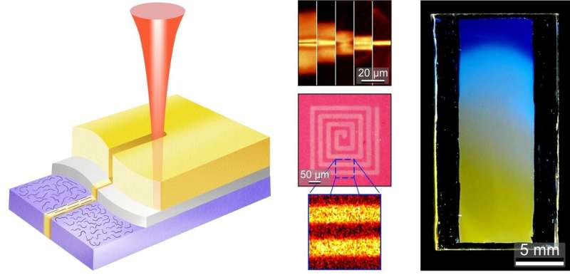
The new method developed by scientists at the Institute of Materials Science of Barcelona (ICMAB-CSIC), Mariano Campoy-Quiles and Aleksandr Perevedentsev, from the Nanostructured Materials for Optoelectronics and Energy Harvesting (Nanopto) group, involves the diffusion of small functional molecules through a 'molecular gate' interlayer before reaching the semiconductor layer, where they induce the desired changes, such as directional polymer chain orientation, enhanced crystallinity, electrical conductivity by doping or modified light emission properties.
"The fact that the method is based on molecular diffusion opens the possibility to modify the composition locally one molecule at a time, thus with extreme compositional accuracy, and that is why we say that our method introduces the concept of 'molecule on demand' into the low-cost, solution-based processing schemes" says Campoy-Quiles.
The diffusion of the small molecules through the molecular gate interlayer is activated by stimuli such as heat, light or vapor jets. When using a focused laser as stimulus, high resolution local patterning of thin-film microstructure and composition is achieved; thus the method can be considered as a bridge between printing and photolithography.
Moreover, the method is inherently rapid and compatible with both serial (e.g. roll-to-roll) and laboratory-scale processing for all types of organic electronic and photonic devices. "One unique trait of this technology—says Campoy—is that it allows to pattern more than one functionality in a single step. One example is the production of pixels exhibiting three different emission colors obtained by the controlled diffusion of several small molecules in the target polymer matrix."
"And the beauty of it," adds Perevedentsev, "is the versatility planted at the root of the concept. We're itching to take it into new territories. Shall we build micro race-tracks for electricity and heat? Can we pattern with electron beams? How about biomolecules? This paper may be the first dot on the map, but it's a long way to the edge!"
The implementation of this method for the fabrication and patterning of semiconducting polymer films, which has been protected by a patent application, could bring organic electronics to the next level, so that flexible and light-weight organic photovoltaics, photonics, transistors and other electronic devices can become competitive with respect to silicon-based electronics.
More information: Aleksandr Perevedentsev et al. Rapid and high-resolution patterning of microstructure and composition in organic semiconductors using 'molecular gates', Nature Communications (2020). DOI: 10.1038/s41467-020-17361-8


