September 24, 2021 feature
A strategy to remotely modulate the doping of 2D transistors

When fabricating electronic devices based on conventional semiconducting materials, engineers need to complete a crucial step known as doping. Doping essentially entails the introduction of impurities into semiconductors to enable the modulation of their optical, electrical, and structural properties.
Although doping is a crucial step in the development of semiconductor-based electronics, many conventional doping strategies introduce too many carriers, leaving ionized dopants behind in the channel and obstructing the transport of charge carriers. Some engineers have thus been trying to devise modulation doping techniques that separate ionized dopants from the channel.
The transport of charge carriers in 2D semiconductors, such as transition metal dichalcogenides (TMDCs) can be influenced by several internal and external factors. In fact, in these materials, carriers are highly confined and affected by scattering effects induced by environmental factors.
Due to this susceptibility to scattering effects, 2D materials have so far proven to be very difficult to study and researchers have not yet fully understood their fundamental physical properties. To study these materials, and particularly to investigate quantum phenomena occurring within them, researchers should thus first eliminate unwanted scattering effects.
Eliminating scattering effects can also increase the performance of devices based on 2D semiconductors, as past studies have found that these effects adversely impact devices' performance and limit their potential for real-world applications. While researchers have proposed several strategies to eliminate external sources of scattering, so far reducing intrinsic scattering that occurs in 2D materials has proven highly challenging.
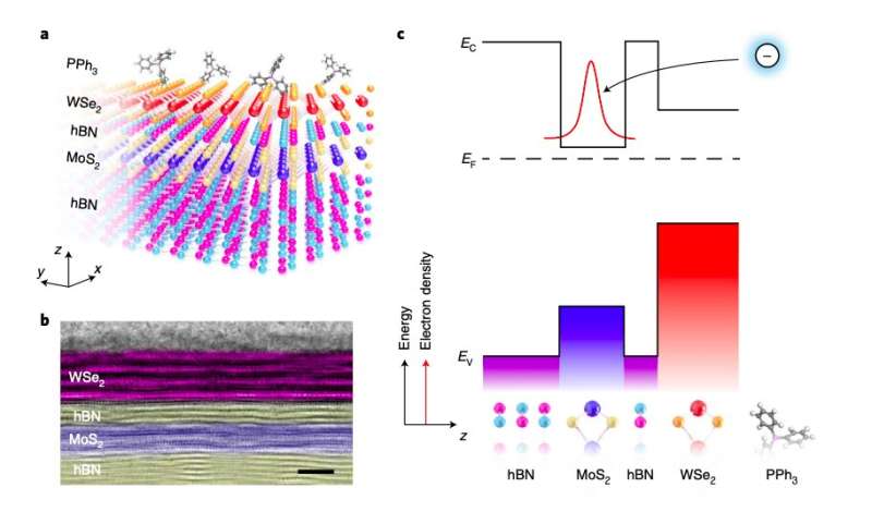
Researchers at Korea University and other institutes in Korea have recently introduced a strategy that could help to reduce intrinsic scattering effects in 2D semiconducting materials. This strategy, presented in a paper published in Nature Electronics, enables the modulation of doping in 2D semiconductors through van der Waals (vdW) band engineering and remote charge transfer doping.
"We report the remote modulation doping of a two-dimensional transistor that consists of a band-modulated tungsten diselenide/hexagonal boron nitride/molybdenum disulfide heterostructure," the researchers wrote in their paper. "The underlying molybdenum disulfide channel is remotely doped via controlled charge transfer from dopants on the tungsten diselenide surface."
Using their doping modulation strategy, the researchers were able to realize a transistor that exhibited a reduced amount of intrinsic scattering. This significantly improved the device's carrier mobility (i.e., how quickly charge carriers can move through the device).
"The modulation-doped device exhibits two-dimensional-confined charge transport and the suppression of impurity scattering, shown by increasing mobility with decreasing temperature," the researchers explained in their paper. "Our molybdenum disulfide modulation-doped field-effect transistors exhibit a room-temperature mobility of 60 cm2 V–1 s–1; in comparison, transistors that have been directly doped exhibit a mobility of 35 cm2 V–1 s–1."
In the future, the study carried out by this team of researchers could pave the way towards the development of faster and more efficient electronics based on semiconductors. In fact, engineers could use the approach presented in the recent paper to control both the carrier mobility and density of 2D field-effect-transistors.
More information: Remote modulation doping in van der Waals heterostructure transistors. Nature Electronics(2021). DOI: 10.1038/s41928-021-00641-6.
© 2021 Science X Network


