Photo-processing of perovskites: Current research status and challenges

The past two decades have seen drastic progress in the development of semiconducting metal-halide perovskites (MHPs). The excellent optoelectronic properties and device performance make perovskites very attractive in various fields.
Photo-processing has been demonstrated to be a facile and general technique for synthesizing perovskites, modifying their structures, and create patterns and devices. This review is of significance to the research and applications of perovskites and also to uncover new views on the light-matter interactions.
As human civilization goes through the information revolution, everything seems to be speeding up, and the desire of researchers to explore next-generation semiconductor materials with excellent optoelectronic properties has significantly increased. The past decades have witnessed a growing interest in metal-halide perovskites due to their impressive optoelectronic properties. This includes significant absorption coefficient, tunable band gap, long carrier diffusion length, low exciton binding energy, and a high defect tolerance.
Metal-halide perovskites have great potential in diverse photovoltaic and optoelectronic devices and applications. In moving from materials to applications, patterning is often an essential part. Due to the low formation energy and ionic crystal structure of metal-halide perovskite, photo-processing can apply as a high-throughput, simple, and chemically clean method of synthesizing, modifying structures, and patterning.
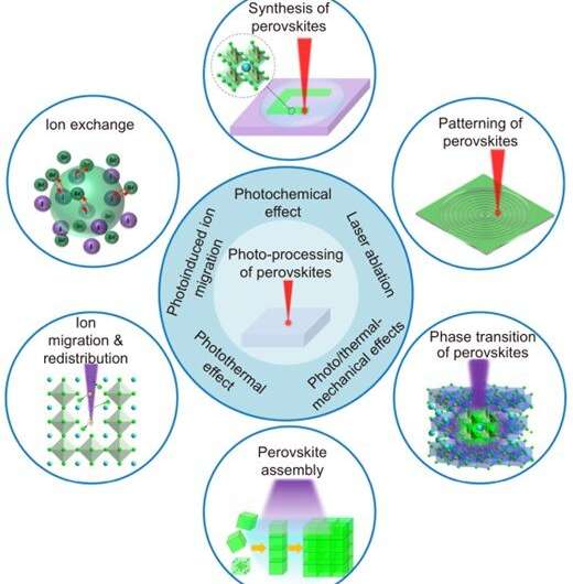
Furthermore, the high mobility of ions (halide ions) offers a unique possibility for the photo-processing of perovskites. It can induce various effects, such as photo-processing of perovskites for synthesis, patterning, ion exchange, phase transition, assembly, and ion migration and redistribution. A more explorative direction for the phenomena and mechanisms of photo-processing will facilitate modulating the optoelectronic properties of perovskite materials.
The authors of the article published in the journal Opto-Electronic Science reviewed the photo-processing for synthesizing perovskites, modifying their structures, and creating patterns & devices.
Photo processing has been established as a powerful technique for material synthesis, structure modification, and patterning in semiconductor science and technology. Compared to other standard processing methods, photo-processing possesses several advantages, such as high area selectivity, compatibility with flexible substrates, and high scalability.
More importantly, direct laser writing is a facile mask-free lithography technique to create desirable and arbitrary patterns, which is crucial for the fabrication of micro-optoelectronic devices.
Photo-processing can induce various effects on the perovskites and the device's performance. Light irradiation can induce serious degradation of the perovskites, generation of defects and phase segregation in mixed-halide perovskites. It can lead to a decrease in the device performance and greatly hinder the application of perovskites. On the contrary, light irradiation can also play a critical and "positive" role in the formation and patterning of perovskites, modifying the structures, tuning the optoelectronic properties and improving the device performance. Light irradiation can induce the generation of perovskites in solution, films and transparent solids. It can enable controlling ion distribution in the perovskites for tuning the bandgap.
Photo-processing has been established as a powerful technique for the synthesis and structure modification of perovskites. In this review, the authors discuss the mechanisms of photo-processing of perovskites and summarize the recent progress in the photo-processing of perovskites for synthesis, patterning, ion exchange, phase transition, assembly, and ion migration and redistribution. The applications of photo-processed perovskites in photovoltaic devices, lasers, photodetectors, light-emitting diodes (LEDs), and optical data storage and encryption are also discussed. Finally, the authors provide an outlook on photo-processing of perovskites and propose promising directions for future researches.
Furthermore, the authors suggest that the typical principles of the photo-processing techniques, such as the photochemical effect, photothermal effect, and laser ablation, is also applicable to other NCs or quantum dots with controlled light sources and precursors. As a result, the discussions in this work will be generally important for the photo-processing of various NCs or quantum dots.
More information: Dezhi Tan et al, Photo-processing of perovskites: current research status and challenges, Opto-Electronic Science (2022). DOI: 10.29026/oes.2022.220014


