December 28, 2022 feature
Re-awakening the world's first solar cells for indoor photovoltaics applications

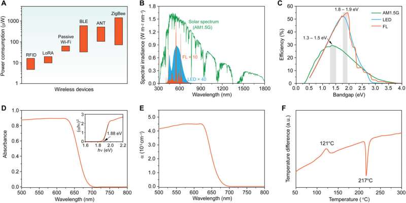
The world's first solid-state photovoltaics were reported in 1883, and were composed of selenium, which eventually led to the development of the present-day photovoltaics, although the wide bandgap of selenium was limiting for applications of sunlight harvesting.
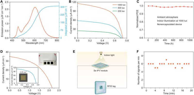
In their present work published in Science Advances, Bin Yan and a team of researchers in chemistry, nanotechnology and materials science in China, revisited the concept of the world's oldest photovoltaics material to describe its role in indoor photovoltaics applications. The adsorption spectrum of the material perfectly matched the emission spectra of commonly used indoor light sources. The researchers used selenium modules to produce an output power of 232.6 μW under indoor light illumination to power a radiofrequency identification-based localization tag.
The field of photovoltaics
In 1873, electrical engineer Willoughby Smith first discovered the photoconductivity of selenium, and Charles Fritts constructed the first solid-state solar cells thereafter in 1883 by sandwiching selenium between a metal foil and a thin gold layer. The low preliminary power conversion efficiency of these early discoveries, initiated research in the field of photovoltaics and inspired the emergence of solar cells in 1954, to lay the foundation to the modern photovoltaic industry.
Until recently, scientists had incorporated indoor photovoltaics to convert indoor light into usable electrical power for wireless devices such as sensors, actuators, and communication devices. In this work, Yan et al. showed the unique advantages of using selenium for indoor photovoltaics with its suitably wide bandgap and intrinsic environmental stability. The team also developed selenium modules to produce an output power of 232.6 μW, to power an internet of things wireless device for radiofrequency identification-based localization.

Indoor photovoltaics
It is now possible to power the "internet of things" devices by harvesting indoor light via indoor photovoltaics (IPV). The concept is a growing research field, where a variety of technologies including dye-sensitized solar cells and organic photovoltaics and lead-halide perovskite solar cells are explored for their functionality.
Indoor light is typically designed to suit human eye sensitivity, so by design its elements differ from conventional outdoor photovoltaics. When the existing features of selenium were combined with its non-toxicity and excellent stability, Yan et al. deemed the material to be ideal for indoor photovoltaic applications.
Optimizing the experiments for improved outcomes
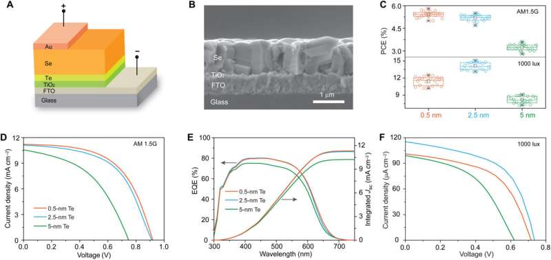
The research team adopted a superstrate configuration of glass/Fluorine-doped tin oxide with titanium oxide/tellurium/selenium and gold to develop the thin-film selenium solar cells. During the process, they used environmentally-friendly titanium oxide to form the buffer layer, and constructed the non-toxic selenium-based devices to facilitate indoor light applications.

During the experiments, they studied the selenium solar cells under standard one-sun illumination and measured indoor photovoltaic performances of devices under indoor light at 1000 Lux, with a common LED source of light to simulate the environment of illumination. The outcomes also led to the optimization of the tellurium layer to facilitate significantly different light intensities between indoor light and sunlight.
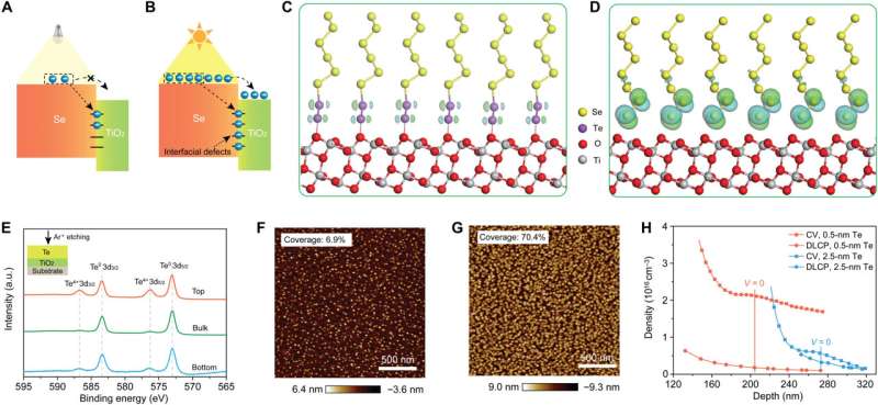
Indoor light could comparatively only generate a relatively small number of carriers on account of its very weak intensity. The team therefore improved the device to obtain a positive photodoping effect to optimize the selenium solar cells under indoor light conditions. Yan et al. additionally incorporated tellurium at the selenium/titanium oxide interface to provide a strong bond for surface passivation.
Applications of the devices
The devices can be used to investigate a range of indoor lighting conditions typically required to light environments such as the living room, the library, or a bright supermarket. The selenium cells outperformed market-dominating silicon-based cells that are presently an industry standard for indoor photovoltaics, relative to both power conversion efficiency and stability.

Contrastingly, silicon-based cells only exhibited a power conversion efficiency below 10%, with relatively minimal photostability. On account of these observations, the team considered the selenium-based devices to be a more attractive alternative candidate. They also studied the capacity of the selenium device to power the internet of things wireless devices.
Outlook
In this way, Bin Yan and colleagues reinterpreted selenium, the oldest existing photovoltaic material with the emergence of indoor photovoltaic devices, due to its unique capacity to offer a suitable wide bandgap for indoor light harvesting. The material is non-toxic and has intrinsic environmental stability as essential features.
The scientists optimized the material composition to achieve a power conversion efficiency of 15%, suited for 1000 Lux indoor illumination with selenium cells. This outcome surpassed the existing efficiency of commercial silicon cells. The selenium devices performed without degradation, even after 1000 hours of continuous indoor lighting.
The outcomes of the study highlight the scope of using selenium for indoor photovoltaics with added potential to power the internet of things devices as an attractive element in photovoltaics.
More information: Bin Yan et al, Indoor photovoltaics awaken the world's first solar cells, Science Advances (2022). DOI: 10.1126/sciadv.adc9923
Richard Haight et al, Solar-powering the Internet of Things, Science (2016). DOI: 10.1126/science.aag0476
© 2022 Science X Network


