Inspecting silicon wafers with terahertz emission spectroscopy could provide new semiconductor options

Silicon (Si) has been the focus of the semiconductor industry and the modern electronic industry for the last half-century. However, its surface properties remain a mystery.
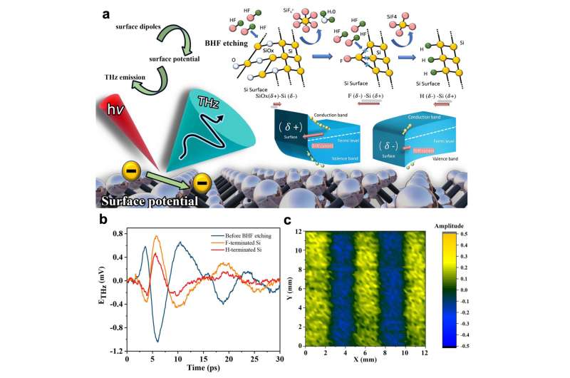
The properties of the Si surface vary widely but are essential to fabricating Si-based devices. Hydrogen fluoride (HF) and its buffered (BHF) solutions are often used to treat the surface and remove the native oxide layer. After BHF etching, a hydrogen(H)-terminated surface forms, and the surface properties change significantly owing to the variation in the surface states and the generation of surface dipoles.
In a new paper published in Light: Science & Applications, a team of scientists led by Professor Masayoshi Tonouchi from Osaka University studied the terahertz (THz) emission properties of Si surfaces. The paper, titled "Rapid, noncontact, sensitive, and semiquantitative characterization of buffered hydrogen-fluoride-treated silicon wafer surfaces by terahertz emission spectroscopy," implied a semiquantitative connection between the THz emission and the surface band bending with the surface dipoles.
Currently, various methods are used to characterize the defects at the wafer surface to confirm a better surface for the photolithography process in the semiconductor industry.
The standard wafer inspection techniques include the brightfield and darkfield inspection by using a laser beam and its reflection at a specific angle, the electron-beam inspection, and the multi-beam inspection by using an electron beam for higher resolution. Besides the defects at the surface of the Si wafer, the surface electric properties are also important to further fabrication and influence the device quality.
To improve the yield of products integrated into the Si wafer, it is essential to characterize the surface properties of the Si wafer rapidly, efficiently, and quantitatively before and after the chemical treatment during the fabrication process. Several useful but complicated tools have been proposed to estimate the surface potential.
These include X-ray photoelectron spectroscopy, surface photovoltage measurement, and Kelvin force microscopy. Methods for sensitive local surface evaluation and rapid surface property mapping are still lacking and urgently needed.
The research team proposed laser-induced terahertz (THz) emission spectroscopy (TES) and laser-induced terahertz emission microscopy (LTEM) as the most promising candidate. These are performed as a sensitive and semiquantitative noncontact local characterization method. It offers an additional mapping function that can efficiently evaluate surface properties, such as surface potential, a passivation layer, and surface charge density.
Ultrafast laser excitation at the surface of a semiconductor generates THz radiation as a result of ultrafast charge transport. The mechanism can be classified mainly into two categories: photocarrier diffusion and the drift of photocarriers. The THz emission from the Si metal–oxide–semiconductor structure is considered to be the combined result of the drift current and diffusion in previous reports. The photo-Dember effect on the bare Si surface is relatively weak compared to the drift current resulting from the surface electric field.
The researchers observe the THz emission from the Si surface before and after removing the native oxide layer using a BHF solution. Meanwhile, the parameters of the doping types and doping concentration also indicate their impact on the observed THz emission waveforms in terms of both amplitude and polarity. The THz waveform's flipping reveals the THz emission's strong dependence on the surface band bending. It is dominated by the surface state energy and Fermi levels in bulk.
Furthermore, the researchers discussed the parameters of the surface properties. They provided an LTEM image of the surface potential distribution on the Si surface with a line-space pattern after BHF etching as an example of the application. LTEM–TES is a promising tool for achieving rapid noncontact and sensitive characterization of Si surface properties and will benefit the modern Si industry.
More information: Dongxun Yang et al, Rapid, noncontact, sensitive, and semiquantitative characterization of buffered hydrogen-fluoride-treated silicon wafer surfaces by terahertz emission spectroscopy, Light: Science & Applications (2022). DOI: 10.1038/s41377-022-01033-x


