This article has been reviewed according to Science X's editorial process and policies. Editors have highlighted the following attributes while ensuring the content's credibility:
fact-checked
peer-reviewed publication
proofread
Large-scale plasma etching technology for mass production of next-generation 2D semiconductors

A large-scale (4-inch), highly uniform, and defect-free plasma etching technology, which will likely become the foundation of the industrial supply of molybdenum disulfide (MoS2), a next-generation two-dimensional (2D) semiconductor, has been developed.
The joint research team led by Hyeong-U Kim, Senior Researcher of the Department of Plasma Engineering at the Korea Institute of Machinery and Materials (KIMM) and Professor Taesung Kim of Sungkyunkwan University, announced that the team has succeeded in developing the "large-scale (4-inch) atomic layer etching technology for MoS2, a next-generation semiconductor, using plasma-based reactive ion etcher (RIE) equipment."
This research, in which senior researcher Muyoung Kim and post-doctoral researcher Changmin Kim of KIMM participated as co-first authors, has been published as the cover article of the February 2023 edition of Chemistry of Materials.
As the line width of conventional silicon-based semiconductors decreases gradually, it is necessary to control the manufacturing process on an atomic level.
However, it is difficult to elaborately process the single-atomic layer of silicon-based semiconductors because of the tunneling effect that occurs during the accumulation of atomic layers. Therefore, it has become a necessity to develop new materials for the advancement of future-generation semiconductors.
Meanwhile, with MoS2, it is possible to stably control the movement of electrons without any tunneling effect, even in a structure that has a thickness of 1 nanometer (nm). Hence, MoS2 has been gaining attention as a promising new material capable of overcoming the limitations of silicon-based semiconductors.
However, although MoS2 has better electric and physical properties compared with silicon even in terms of atomic layer thickness, the development of MoS2-based semiconductors has remained at the basic research stage in laboratories because of the difficulty of forming MoS2 uniformly in large scales for mass manufacturing.
In particular, while it is necessary to form a layer that has the thickness of a single atom in order to achieve the precision of semiconductors, the possibility of commercialization of MoS2 was not proven due to the lack of the technology for precisely etching MoS2 into atomic layers.
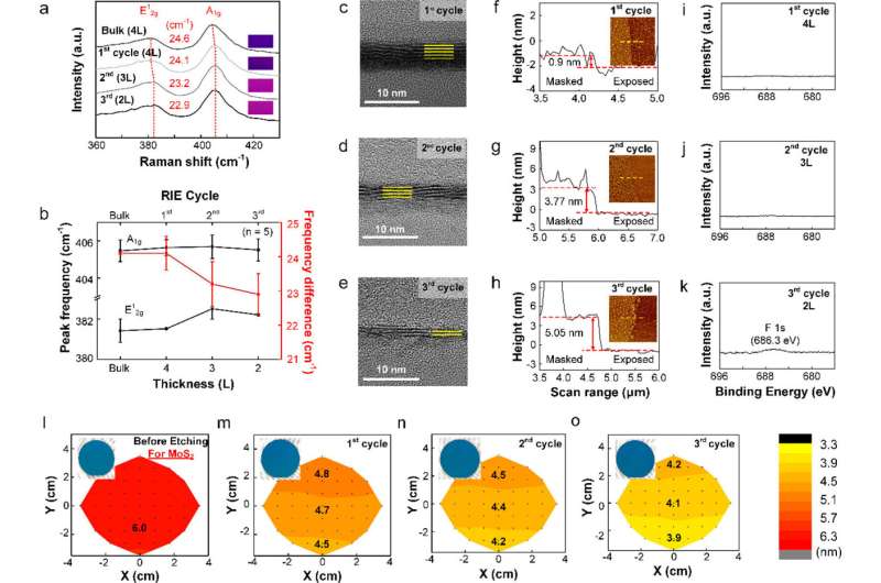
In this research, a process, that enables the etching of large-scale (4-inch) MoS2 to the desired atomic layer thickness using the two plasma processes of plasma-enhanced chemical vapor deposition (PECVD) and RIE, has been developed for the first time. As a result, the research has opened new horizons for the industrial utilization of MoS2-based semiconductors.
Plasma etching process has gained huge attention as the most probable technology that could break the limits of conventional etching process. However, one of the major downsides of plasma etching is that impurities (fluorine, F) remain on the surface of the semiconductor after the process, and therefore, additional steps are necessary to remove such residues. For this reason, highly sophisticated design of plasma process was a long-standing desire to satisfy both atomic-level precision and ultrahigh purity in MoS2 layers.
In the latest study, the research team resolved such issues by adopting a computational screening system based on the density functional theory (DFT). Muyoung Kim, Ph.D., one of the co-first authors, proposed the state-of-the-art computational screening system that simulated surface reaction of candidate gases and combined the best gas mixture for ultrafine process quality. One crucial advancement of this approach is that the screening system greatly reduces the development time and cost of plasma process, compared to the conventional experiment-based manufacturing. In particular, he examined atomistic mechanism of surface reaction and identified the role of process gas on MoS2 substrate, which rationalized the mixed-gas recipe (Ar + O2 + CF4).
Senior Researcher Hyeong-U Kim of KIMM who led the research said, "future industries such as AI, GPT, IoT, self-driving, and cloud, etc. all fall under the category of non-memory sectors. Accordingly, even Samsung Electronics, the leader of the memory market, has also been focusing its investments on the foundry sector. The manufacturing process of semiconductor memories has focused on the mass production of limited items, while the foundry process seeks limited production of diverse items. Hence, processes capable of controlling delicate line widths have become increasingly important, especially in the foundry process."
Kim added, "To overcome the limitations of integration, it is necessary to develop processes where even single-atomic layers are controllable, as demonstrated in our latest research. Hence, many studies have been conducted since around a decade ago. However, before our latest study, no researcher has been able to demonstrate the possibility of etching atomic layers uniformly and reproducibly in a large scale. Our research outcome is expected to help the next-generation 2D semiconductor industry in the non-memory sector to find a new breakthrough in the future."
More information: Changmin Kim et al, First-Principles Calculation Guided High-Purity Layer Control of 4 in. MoS2 by Plasma RIE, Chemistry of Materials (2023). DOI: 10.1021/acs.chemmater.2c02914


