October 11, 2023 feature
This article has been reviewed according to Science X's editorial process and policies. Editors have highlighted the following attributes while ensuring the content's credibility:
fact-checked
peer-reviewed publication
trusted source
proofread
A new reconfigurable field-effect transistor and memory device based on a 2D heterostructure

Transistors are crucial components of most electronics on the market today, including computers, smartphones, wearables and numerous other devices. These components, generally based on semiconducting materials, are designed to switch, detect and amplify current inside devices, controlling the flow of electricity inside them during their operation.
As conventional transistors are reaching their highest possible performance, electronics engineers have been working on alternative transistor designs that could be promising for future applications. Using different materials and arranging these materials in unique ways, engineers hope to enhance the performance of transistors, reduce their size or enable unique functions.
Reconfigurable field-effect transistors (FETs) are an emerging class of transistors that could help to reduce the complexity of electronics, by combining different functions in a single device. Specifically, these programmable transistors could combine the characteristics of unipolar n- and p-type semiconductors.
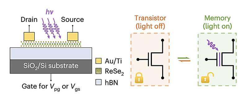
Researchers at National Tsing Hua University, National Chung Hsing University and other institutes in China recently a new reconfigurable device based on a 2D heterostrucure that can serve as a transistor and memory. This transistor, published in Nature Electronics, can be modulated via a photo-induced trapping mechanism.
"Current reconfigurable FETs require a constant voltage supply to achieve polarity conversion, leading to high power consumption," Meng-Yu Tsai, Chia-Tse Huang and their colleagues wrote in their paper. "We report a reconfigurable FET that is based on a hexagonal boron nitride/rhenium diselenide/hexagonal boron nitride (hBN/ReSe2/hBN) heterostructure and has a non-volatile and tunable polarity."
The properties and characteristics of the researchers' reconfigurable transistor can be modulated via a light-induced mechanism known as photoinduced trapping. Using this method, the team was able to reversibly control the holes/electrons trapped at the interface between hBN and SiO2 inside the device, in turn modulating the device's channel doping configuration.
The unique design introduced by Tsai, Huang and their colleagues results in a transistor that can span multiple different charge transport regimes. This transistor could ultimately be advantageous for a broad range of electronics applications, as it could help to boost the performance of both computing and memory devices.
"A photoinduced trapping mechanism is used to drive photoexcited holes or electrons into the interface between the hBN and the silicon dioxide substrate," Tsai, Huang and their colleagues wrote in their paper. "The reconfigurable FET can switch between a transistor and memory mode, and several FETs can be used to create inverter, AND, OR, NAND, NOR, XOR and XNOR circuits. We also show that, when in memory-mode operation, the devices can be used to emulate synaptic functions for neuromorphic computing systems."
In their paper, Tsai, Huang and their colleagues demonstrate the potential of using their transistor to boost and broadening the functionalities of logic circuits. Its performance could be further explored and validated in their future works.
In the future, the team's reconfigurable transistor could also prove valuable for the development of highly performing circuits for neuromorphic computing applications. These are hardware systems designed to replicate the organization and functions of biological neural circuits in the brain.
More information: Meng-Yu Tsai et al, A reconfigurable transistor and memory based on a two-dimensional heterostructure and photoinduced trapping, Nature Electronics (2023). DOI: 10.1038/s41928-023-01034-7
© 2023 Science X Network


