This article has been reviewed according to Science X's editorial process and policies. Editors have highlighted the following attributes while ensuring the content's credibility:
fact-checked
trusted source
proofread
Better microelectronics from coal

Coal is an abundant resource in the United States that has, unfortunately, contributed to climate change through its use as a fossil fuel. As the country transitions to other means of energy production, it will be important to consider and reevaluate coal's economic role.
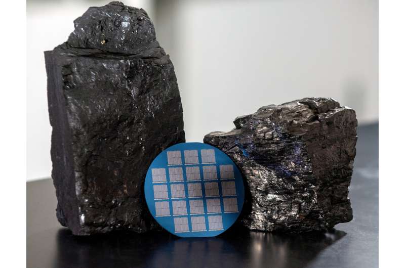
A joint research effort from the University of Illinois Urbana-Champaign, the National Energy Technology Laboratory, Oak Ridge National Laboratory and the Taiwan Semiconductor Manufacturing Company has shown how coal can play a vital role in next-generation electronic devices.
"Coal is usually thought of as something bulky and dirty, but the processing techniques we've developed can transform it into high-purity materials just a couple of atoms thick," said Qing Cao, a U. of I. materials science & engineering professor and a co-lead of the collaboration. "Their unique atomic structures and properties are ideal for making some of the smallest possible electronics with performance superior to state-of-the-art."
A process developed by the NETL first converts coal char into nanoscale carbon disks called "carbon dots" that the U. of I. research group demonstrated can be connected to form atomically thin membranes for applications in both two-dimensional transistors and memristors, technologies that will be critical to constructing more advanced electronics. These results are reported in the journal Communications Engineering.
Perfect for 2D electronics
In the ongoing search for smaller, faster, and more efficient electronics, the final step will be devices made with materials just one or two atoms thick. It is impossible for devices to be smaller than this limit, and their small scale often makes them operate much quicker and consume far less energy.
While ultrathin semiconductors have been extensively studied, it is also necessary to have atomically thin insulators—materials that block electric currents—to construct working electronic devices like transistors and memristors.
Atomically thin layers of carbon with disordered atomic structures can function as an excellent insulator for constructing two-dimensional devices. The researchers in the collaboration have shown that such carbon layers can be formed from carbon dots derived from coal char. To demonstrate their capabilities, the U. of I. group led by Cao developed two examples of two-dimensional devices.
"It's really quite exciting because this is the first time that coal, something we normally see as low-tech, has been directly linked to the cutting edge of microelectronics," Cao said.
Transistor dielectric
Cao's group used coal-derived carbon layers as the gate dielectric in two-dimensional transistors built on the semimetal graphene or semiconductor molybdenum disulfide to enable more than two times faster device operating speed with lower energy consumption. Like other atomically thin materials, the coal-derived carbon layers do not possess "dangling bonds" or electrons that are not associated with a chemical bond.
These sites, which are abundant on the surface of conventional three-dimensional insulators, alter their electrical properties by effectively functioning as "traps," slowing down the transport of mobile charges and, thus, the transistor switching speed.
However, unlike other atomically thin materials, the new coal-derived carbon layers are amorphous, meaning that they do not possess a regular, crystalline structure. They, therefore, do not have boundaries between different crystalline regions that serve as conduction pathways leading to "leakage," where undesired electrical currents flow through the insulator and cause substantial additional power consumption during device operations.
Memristor filament
Another application Cao's group considered is memristors—electronic components capable of both storing and operating on data to enhance the implementation of AI technology greatly. These devices store and represent data by modulating a conductive filament formed by electrochemical reactions between a pair of electrodes with the insulator sandwiched in between.
The researchers found that adopting ultrathin coal-derived carbon layers as the insulator allows the fast formation of such filament with low energy consumption to enable high device operating speed with low power. Moreover, atomic size rings in these coal-derived carbon layers confine the filament to enhance the reproducible device operations for enhanced data storage fidelity and reliability.
From research to production
The new devices developed by the Cao group provide proof-of-principle for using coal-derived carbon layers in two-dimensional devices. What remains is to show that such devices can be manufactured on large scales.
"The semiconductor industry, including our collaborators at Taiwan Semiconductor, is very interested in the capabilities of two-dimensional devices, and we're trying to fulfill that promise," Cao said. "Over the next few years, the U. of I. will continue collaborating with NETL to develop a fabrication process for coal-based carbon insulators that can be implemented in industrial settings."
More information: Fufei An et al, Ultrathin quasi-2D amorphous carbon dielectric prepared from solution precursor for nanoelectronics, Communications Engineering (2023). DOI: 10.1038/s44172-023-00141-9


