April 1, 2024 feature
This article has been reviewed according to Science X's editorial process and policies. Editors have highlighted the following attributes while ensuring the content's credibility:
fact-checked
peer-reviewed publication
trusted source
proofread
Using a 2D perovskite oxide as a photoactive high-κ gate dielectric

Two-dimensional (2D) superconducting materials have been found to be promising for the development of miniaturized optoelectronic devices. To perform well while consuming less energy, however, these smaller devices require a higher gate capacitance (i.e., gates that can store more electrical charge in proportion to the voltage applied).
One approach to boost gate capacitance without decreasing the thickness of gate insulators or gate dielectrics entails the use of insulating materials with a high dielectric constant (κ), such as hafnium oxide (HfO2). While this could be an advantageous solution, these materials have proved to be difficult to integrate with 2D semiconductors.
Researchers at Fudan University recently prepared a 2D perovskite oxide with high-κ that can be integrated with different 2D channel materials. Their paper, published in Nature Electronics, could open new opportunities for the future down-scaling of optoelectronics.
"High dielectric constant (high-κ) gate dielectrics compatible with two-dimensional (2D) semiconductors are essential for scaled optoelectronic devices," Siyuan Li, Xinya Liu and their collaborators wrote in their paper.
"However, conventional three-dimensional dielectrics are difficult to integrate with 2D materials with dangling-bond-free surfaces. We show that the 2D perovskite oxide Sr2Nb3O10, prepared by a top-down approach, can be integrated with various 2D channel materials."
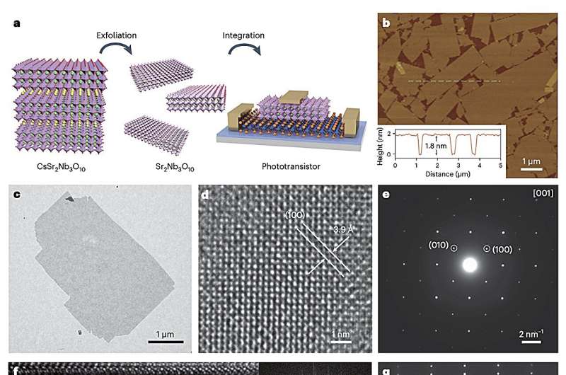
Sr2Nb3O10, the 2D perovskite oxide introduced in the researchers' paper, was synthesized following a top-down preparation strategy. After they prepared SNO nanosheets, they were able to transfer them onto various 2D materials.
Notably, Sr2Nb3O10 exhibits a high κ of 24.6 and a moderate bandgap. These advantageous characteristics enable its use as a photoactive high-κ dielectric for phototransistors based on various 2D semiconducting materials, including graphene, molybdenum disulfide, tungsten disulfide and tungsten diselenide.
To evaluate the promise of their synthesized 2D perovskite oxide for developing miniaturized optoelectronics, the researchers transferred it onto various channel materials, including molybdenum disulfide and tungsten disulfide. They then tested the performance of transistors integrating these materials with Sr2Nb3O10.
"Molybdenum disulfide transistors exhibit an on/off ratio of 106 with a supply voltage of 2 V and a subthreshold swing of 88 mV dec−1," Li, Liu and their colleagues wrote in their paper.
"Tungsten disulfide phototransistors exhibit a photocurrent-to-dark-current ratio of ~106 and ultraviolet (UV) responsivity of 5.5 × 10³ A W−1 under visible or UV light illumination, due to the combined effect of gate control and charge transfer from the photoactive gate dielectric."
The initial findings gathered by this team of researchers were highly promising, as they could successfully integrate their perovskite oxide with various channel materials following a simple procedure. Moreover, the well-defined interface established between the semiconductor and dielectric, along with the high-κ of Sr2Nb3O10, were found to enable the efficient gate control of channel materials.
"We also show that the phototransistors with the photoactive dielectric can offer UV-visible dual-band photodetection, where UV and visible light illumination are distinguished at separate terminals," the researchers wrote in their paper.
This recent work by Li, Liu and their collaborators could soon pave the way for the synthesis of additional 2D perovskite oxides that can be integrated with existing semiconductors and channel materials. Collectively these 2D perovskite oxides could be used to develop smaller, better performing, and energy-efficient electronics or optoelectronics.
More information: Siyuan Li et al, Two-dimensional perovskite oxide as a photoactive high-κ gate dielectric, Nature Electronics (2024). DOI: 10.1038/s41928-024-01129-9.
© 2024 Science X Network


