February 20, 2024 feature
This article has been reviewed according to Science X's editorial process and policies. Editors have highlighted the following attributes while ensuring the content's credibility:
fact-checked
peer-reviewed publication
trusted source
proofread
An architecture for sub-picowatt logic computing based on self-biased molybdenum disulfide transistors

The continuous improvement of circuits and electronic components is vital for the development of new technologies with enhanced capabilities and unique characteristics. In recent years, most electronics engineers have been specifically focusing on reducing the size of transistors, while retaining a low power consumption.
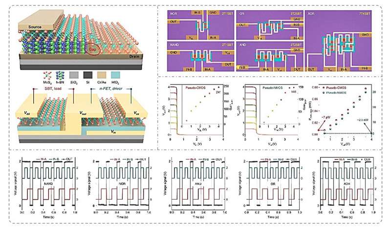
Researchers at University of Science and Technology Beijing recently introduced a new pseudo-CMOS architecture based on self-biased molybdenum disulfide transistors. This architecture, outlined in Nature Electronics, could be used to create highly performing inverters, gate circuits, and other device components.
"The development of integrated circuits (ICs) for efficient computing with low power is a global hot topic and a focus of international competition in cutting-edge fields," Zheng Zhang, co-author of the paper, told Tech Xplore.
"Two-dimensional (2D) materials, such as monolayer molybdenum disulfide (MoS2), have stable structures that can break through the physical limit of downscaling dimensions, excellent field-effect properties, and immunity to short channel effects, making them one of the most promising channel materials for low-power ICs."
Despite their advantageous structure, 2D materials aligned with conventional silicon-based circuit designs (namely, CMOS and NMOS) have been found to exhibit significant limitations. Specifically, the limited polarity control of their atomically thin structure poses challenges for realizing their potential in transistor designs.
Zhang and his colleagues set out to design an alternative, pseudo-CMOS architecture for ultra-low-power logic computing using 2D materials. Their hope was to open new avenues for the development of future ICs.
"Our pseudo-CMOS logic devices are implemented by connecting self-biased transistors (SBTs) as the load and n-type field-effect transistors (n-FETs) as the driver in series," Zhang explained. "The homogeneous SBT with a gap barrier can timely cut off the current path (less than 1 pA) of device when the n-FET is on, thus achieving picowatt-level static power, which is only about 1% and 0.3% of the CMOS and NMOS logic device, respectively."
By combining pass-transistor logic (PTL) designs, the new architecture introduced by the researchers was found to reduce the number of transistors in circuits by 80% compared to conventional IC architectures. In contrast with previously introduced CMOS and NMOS 2D material–based electronics, the team's architecture circumvents the polarity control of transistors, greatly reducing their static power.
"The implementation of the general Boolean functions (i.e., XOR, AND, OR, NAND, NOR and NOT gates) based on pseudo-CMOS architecture opens a scalable pathway toward low-power ICs based on 2D materials," Zhang said. "Our findings solve the key challenge that 2D materials cannot effectively restrain the rapidly rising static power due to the limited polarity control technology."
The architecture introduced by Zhang and his colleagues could serve as an inspiration for other research groups, potentially leading to the creation of new electronics with low power consumption and fast operating speeds. The researchers already used their design to create a prototype inverters and gate circuits for sub-picowatt logic computing, both of which attained very promising results.
"In future work, we plan to develop large-scale ICs of this technology, including various complex combination circuits and sequential circuits based on pseudo-CMOS architecture," Zhang added. "This could enable the implementation of virtually any digital ICs to promote the industrial application of 2D materials."
More information: Xiaofu Wei et al, Homojunction-loaded inverters based on self-biased molybdenum disulfide transistors for sub-picowatt computing, Nature Electronics (2024). DOI: 10.1038/s41928-023-01112-w
© 2024 Science X Network


