This article has been reviewed according to Science X's editorial process and policies. Editors have highlighted the following attributes while ensuring the content's credibility:
fact-checked
peer-reviewed publication
trusted source
proofread
Engineers develop technique to pinpoint nanoscale 'hot spots' in electronics to improve their longevity

When electronic devices like laptops or smartphones overheat, they are fundamentally suffering from a nanoscale heat transfer problem. Pinpointing the source of that problem can be like trying to find a needle in a haystack.
"The building blocks of our modern electronics are transistors with nanoscale features, so to understand which parts of overheating, the first step is to get a detailed temperature map," says Andrea Pickel, an assistant professor from the University of Rochester's Department of Mechanical Engineering. "But you need something with nanoscale resolution to do that."
Existing optical thermometry techniques are impractical because they have fundamental limits on the spatial resolution they can achieve.
So Pickel and materials science Ph.D. students Ziyang Ye and Benjamin Harrington engineered a new approach to overcome these limitations by leveraging Nobel Prize in Chemistry–winning optical super-resolution fluorescence microscopy techniques used in biological imaging.
In a new Science Advancesstudy, the researchers outline their process for mapping heat transfer using luminescent nanoparticles.
By applying highly doped upconverting nanoparticles to the surface of a device, the researchers were able to achieve super-high resolution thermometry at the nanoscale level from up to 10 millimeters away. According to Pickel, that distance is extremely far in the world of super-resolution microscopy and that the biological imaging techniques they used for inspiration typically operate less than one millimeter away.
-
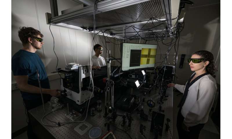
Department of Mechanical Engineering Assistant Professor and Laboratory for Laser Energetics (LLE) scientist Andrea Pickel (right), assistant professor of mechanical engineering at the University of Rochester and her materials science Ph.D. students Benjamin Harrington (left) and Ziyang Ye developed new techniques for mapping heat transfer in electronic devices using luminescent nanoparticles. Credit: University of Rochester / J. Adam Fenster -

Materials science Ph.D. student Benjamin Harrington uses a wire bonder to add electrical connections to an electrical heater structure. The structure was designed as a test subject for a new heat mapping technique that leverages Nobel Prize in Chemistry–winning optical super-resolution fluorescence microscopy techniques. Credit: University of Rochester / J. Adam Fenster
Pickel says that while the biological imaging techniques provide great inspiration, applying them to electronics had significant hurdles because they involve such different materials.
"Our requirements are very different from biologists because they're looking at things like cells and water-based materials," she says. "Often, they might have a liquid like water or an oil between their objective lens and their sample. That's great for biological imaging, but if you're working with an electronic device, that's the last thing you want."
The paper demonstrates the technique using an electrical heater structure that the team designed to produce sharp temperature gradients, but Pickel says their method can be used by manufacturers to improve a wide array of electrical components. To further improve the process, the team hopes to lower the laser power used and refine the methods for applying layers of nanoparticles to the devices.
More information: Andrea Pickel, Optical Super-Resolution Nanothermometry via Stimulated Emission Depletion Imaging of Upconverting Nanoparticles, Science Advances (2024). DOI: 10.1126/sciadv.ado6268. www.science.org/doi/10.1126/sciadv.ado6268


