October 1, 2015 report
New flat transistor defies theoretical limit

A team of researchers with members from the University of California and Rice University has found a way to get a flat transistor to defy theoretical limitations on Field Effect Transistors (FETs). In their paper published in the journal Nature, the team describes their work and why they believe it could lead to consumer devices that have both smaller electronics and longer battery life. Katsuhiro Tomioka with Erasmus MC University Medical Center in the Netherlands offers a News & Views article discussing the work done by the team in the same journal edition.
As Tomioka notes, the materials and type of architecture currently used in creating small consumer electronic devices is rapidly reaching a threshold upon which a tradeoff will have to be made—smaller transistors or more power requirements—this is because of the unique nature of FETs, shortening the channel they use requires more power, on a logarithmic scale. Thus, to continue making FETs ever smaller and to get them to use less power means two things, the first is that a different channel material must be found, one that allow high switch-on currents at low voltages. The second is a way must be found to lower the voltage required for the FETs.
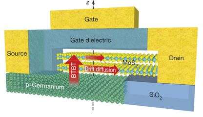
Researchers have made inroads on the first requirement, building FETs with metal-oxide-semiconductor materials, for example. The second has proved to be more challenging. In this latest effort, the researchers looked to tunneling to reduce voltage demands, the results of which are called, quite naturally, tunneling FETs or TFETs—they require less voltage because they are covered (by a gate stack) and work by transporting a charge via quantum-tunneling. The device the team built is based on a 2D bilayer of molybdenum disulfide and bulk germanium—it demonstrated a negative differential resistance, a marker of tunneling, and a very steep subthreshold slope (the switching property associated with rapid turn-on) which fell below the classical theoretical limit.
The work by the team represents substantial progress in solving the minituration problem for future electronics devices, but as the team notes, there is still much to do. They express optimism that further improvements will lead to not just better consumer devices, but tiny sensors that could be introduced into the body to help monitor health.
More information: A subthermionic tunnel field-effect transistor with an atomically thin channel, Nature 526, 91–95 (01 October 2015) DOI: 10.1038/nature15387
Abstract
The fast growth of information technology has been sustained by continuous scaling down of the silicon-based metal–oxide field-effect transistor. However, such technology faces two major challenges to further scaling. First, the device electrostatics (the ability of the transistor's gate electrode to control its channel potential) are degraded when the channel length is decreased, using conventional bulk materials such as silicon as the channel. Recently, two-dimensional semiconducting materials have emerged as promising candidates to replace silicon, as they can maintain excellent device electrostatics even at much reduced channel lengths. The second, more severe, challenge is that the supply voltage can no longer be scaled down by the same factor as the transistor dimensions because of the fundamental thermionic limitation of the steepness of turn-on characteristics, or subthreshold swing. To enable scaling to continue without a power penalty, a different transistor mechanism is required to obtain subthermionic subthreshold swing, such as band-to-band tunnelling. Here we demonstrate band-to-band tunnel field-effect transistors (tunnel-FETs), based on a two-dimensional semiconductor, that exhibit steep turn-on; subthreshold swing is a minimum of 3.9 millivolts per decade and an average of 31.1 millivolts per decade for four decades of drain current at room temperature. By using highly doped germanium as the source and atomically thin molybdenum disulfide as the channel, a vertical heterostructure is built with excellent electrostatics, a strain-free heterointerface, a low tunnelling barrier, and a large tunnelling area. Our atomically thin and layered semiconducting-channel tunnel-FET (ATLAS-TFET) is the only planar architecture tunnel-FET to achieve subthermionic subthreshold swing over four decades of drain current, as recommended in ref. 17, and is also the only tunnel-FET (in any architecture) to achieve this at a low power-supply voltage of 0.1 volts. Our device is at present the thinnest-channel subthermionic transistor, and has the potential to open up new avenues for ultra-dense and low-power integrated circuits, as well as for ultra-sensitive biosensors and gas sensors.
© 2015 Tech Xplore


