Novel semiconductor-superconductor structure features versatile gallium nitride

Silicon has been the semiconductor material of choice for electronics pretty much since the transistor effect was first observed and identified nearly 80 years ago. There's a valley in California named for it, after all.
But a relatively new family of semiconductors – group III-nitrides, including gallium nitride (GaN), indium nitride and aluminum nitride – offers greater versatility than silicon with capabilities for ultrafast wireless communications, high-voltage switches and high intensity lighting and photonics.
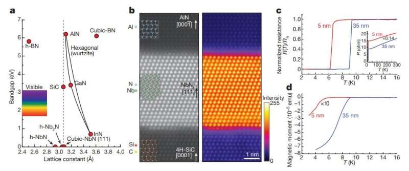
A team led by Debdeep Jena, professor of electrical and computer engineering (ECE), and David Meyer, head of the Wide Bandgap Materials and Devices section at the Naval Research Laboratory, has successfully devised a semiconductor-superconductor crystal structure featuring GaN grown directly onto a crystal of niobium nitride (NbN), a proven superconductor material used in quantum communications, astronomy and a host of other applications.
The group's paper, "GaN/NbN Epitaxial Semiconductor/Superconductor Heterostructures," is being published online March 8 in Nature. Former postdoctoral researcher Rusen Yan and current postdoc Guru Khalsa are co-lead authors.
Other key contributors were Grace Xing, the Richard Lundquist Sesquicentennial Professor in ECE and MSE, and David Muller, the Samuel B. Eckert Professor of Engineering in the Department of Applied and Engineering Physics.
The method for combining the two materials – molecular beam epitaxy (MBE), essentially spray painting of gallium and nitrogen atoms onto the NbN in a vacuum environment – creates an extremely clean interface and is key to the success of the novel structure.
This advance, the group says, opens up a range of possibilities that can now combine the macroscopic quantum effects of superconductors with the rich electronic and photonic properties of group III-nitride semiconductors.
"People have tried it with other semiconductors, like silicon and gallium arsenide, but I don't think anything has been as successful as what we've managed to do with GaN," said Jena, who has a dual appointment with the Department of Materials Science and Engineering (MSE).
Gallium nitride-based semiconductors have recently made major inroads in the areas of LED lighting, Blu-ray laser diodes, energy and communications. In fact, the 2014 Nobel Prize in physics was given to a trio of Japanese scientists for their invention of energy-efficient blue light-emitting diodes (LEDs) using GaN.
Technological advances – particularly the type of MBE used in this work, which was developed at the Naval Research Laboratory – has made it possible for scientists to think about semiconductor-superconductor heterostructures such as the one Jena's group has developed.
The specialized nitride MBE system includes an electron beam evaporator source, which "melts" the niobium – which has a melting point of around 4,500 degrees – but not the crucible it's in. Atoms of niobium are deposited onto a silicon carbide wafer, and the GaN semiconductor layers are then grown on top of that, also by MBE.
"This new source allowed us to overcome the temperature limitations of conventional sources, and bring high-melting-point, refractory transition metals like niobium and tantalum into the picture," Meyer said.
The team demonstrated for the first time the growth and fabrication of a semiconductor transistor switch, the prototypical gain element in electronics, directly on top of a crystalline superconductor layer. This heterostructure is a kind of "best of both worlds," Jena said, offering a method for devising quantum computation and highly secure communications systems.
"There are some things that we would love to do with quantum systems – quantum computation and cryptography, things that are not possible in classical systems," he said. "On the other hand, there are things that classical systems are much better at than quantum systems. And there is this mesozone where you can do wonderful things by mixing and matching the two."
"We think this presents a wonderful opportunity for rapid technology development of next-generation communications and computation systems," Meyer said.
More information: Rusen Yan et al. GaN/NbN epitaxial semiconductor/superconductor heterostructures, Nature (2018). DOI: 10.1038/nature25768


