May 18, 2019 weblog
Samsung at foundry event talks about 3nm, MBCFET developments

"The nanometer process deals with the space between the transistors mounted on a substrate at a nanometer level," said Pulse.
"The narrower the distance, the more chips can be squeezed in to boost computing power and energy efficiency. One nanometer corresponds to one ten-thousandth the diameter of a human hair."
At the Samsung Foundry Forum in Santa Clara, California, the company recently sought to impress advancements it has made in 3nm gate-all-around (GAA) process development.
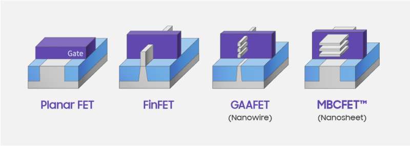
Samsung Foundry now introduces MBCFET (multi bridge channel FET). This consists of multi-stacked nanosheets. With the nanosheet formation, a larger current per stack is achievable, said SamMobile.
ExtremeTech described the announcement as being about "a new, evolved transistor architecture" coming out of Samsung Foundry—involving the "nanosheets" approach for its 3nm node.
(From Samsung's newsroom: "Conventional GAA based on nanowire requires a larger number of stacks due to its small effective channel width. On the other hand, Samsung's patented version of GAA, MBCFET (Multi-Bridge-Channel FET), uses a nanosheet architecture, enabling greater current per stack.")
The blog CNXSoft further shed light on why the transition from nanowires to nanosheets.
"We often read new processor are manufactured with a FinFET process. The new process was created due to short channel effects in traditional planar transistors, and FinFET (Fin Field-effect transistor) was introduced to enable further voltage scaling but with the process node becoming smaller and smaller, electrostatics effects started to cause problem."
Using GAA (Gate All Around) nanowires to limit those effects was taken as an answer, but those are apparently really hard to integrate into silicon, said the blog, so Samsung ended up using thin layers (nanosheets) instead of nanowires, "enabling greater current per track in their GAA implementation called MBCFET (Multi-Bridge Channel Field-Effect Transistor)."
For those who need to process the overload of acronyms, Ramish Zafar in Wccftech took his readers along the Samsung journey. 1. Samsung collaborated with IBM for GAAFET (Gate-All-Around) process nodes. 2. Now the company has announced its customizations to the earlier process, and this is MBCFET.
Zafar had more to say about MBCET. "As opposed to traditional FinFET designs, GAAFET allows the gate material to surround the channel from all sides. Samsung claims that MBCFET's design will improve the process' on-off behavior, and allow processors to reduce operational voltage below 0.75V. A crucial point for MBCFET is that the process is fully compatible with FinFET designs and does not require any new tools for manufacturing."

How, though, does all this good-news figure into the company development plans. When can we expect to see technology in action? Joel Hruska addressed this in ExtremeTech.
"At its Samsung Foundry Forum this week, Samsung declared that its Product Design Kit for 3nm chips is now in alpha, having reached the 0.1 development milestone. Samsung is planning to launch a plethora of process nodes in the coming years, with development tracks planned for 7nm, 6nm, 5nm, 4nm, and yes, 3nm."
Hruska added, "The improvements for 3nm compared to 7nm are fairly good, but this node won't actually ship for quite some time." His article carries a chart that shows the progression as communicated by Samsung.
© 2019 Science X Network


