November 20, 2019 feature
Hourglass-shaped silicon photodiodes with an enhanced near-infrared photoresponse

Silicon photodiodes are semiconductor devices commonly used to detect visible light and measure its intensity, color and position. The fact that these devices are made of silicon has both advantages and disadvantages.
Although silicon can be used to develop systems that are cheaper and fairly easy to integrate with read-out electronics, it also prevents photodiodes from detecting near-infrared (NIR) and short-wave infrared (SWIR) light. In fact, silicon has a bandgap of 1.12 eV, which is equivalent to a wavelength of 1,100nanometer. This ultimately makes it difficult for photodiodes made of silicon to detect NIR light (at wavelengths of 700 to 1,000 nanometer) and SWIR light (at wavelengths of 1,000 to 1,700 nanometer).
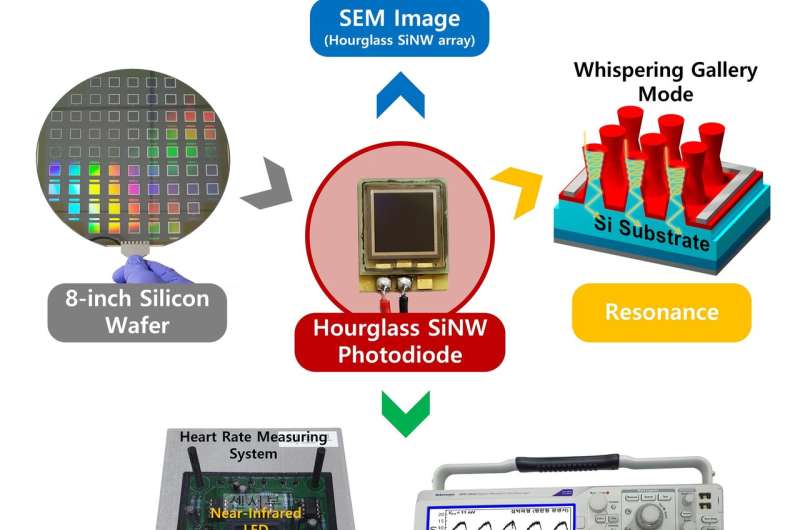
To overcome this limitation, a team of researchers at Pohang University of Science and Technology (POSTECH) and the NASA Ames Research Center has recently developed a new type of silicon photodiodes based on hourglass-shaped silicon nanowires with whispering gallery modes that enhance their near-infrared photoresponse. Their study was featured in Nature Electronics.
"The starting point of this research was to develop a silicon photodetector for power monitoring of laser surgical equipment using a 1,064-nanometer light source (mainly used for ophthalmic applications, etc.)," Chang-Ki Baek, one of the researchers who carried out the study, told TechXplore.

Initially, Baek and his colleagues tried to optimize the absorption of 1,064-nanometer wavelength light by changing the diameter and height of inverted-cone-shaped silicon nanowire (SiNW) structures that their lab had previously developed. To do this, they adjusted the etching gas ratio and etching time of a HBr HBr / Cl2 / O2 mixture.
This led to the unexpected appearance of the first hourglass-shaped SiNW array in certain O2 gas conditions. In their previous research, the researchers observed two key optical properties of cone-shaped SiNW structures: an increasing light absorption in inverted-cone-shaped structures resulting from their resonance, and a decreasing surface reflectance in regular cone-shaped structures due to their refractive index matching.
"Since the hourglass-shaped SiNW has the advantages of both inverted and straight cone-shaped structures, we predicted that applying an hourglass-shaped SiNW array to photodiode would improve the near-infrared detection," Baek said. "In TCAD simulations and experiments, we verified the improvement of near-infrared detection with the fabricated photodiode. As a result, our hourglass-shaped SiNW photodiode can be expressed as an unintentionally discovered idea during the design of an etching process."
The device proposed by the researchers is the most basic type of PN junction photodiode. It was fabricated employing methods that are commonly used to make silicon semiconductors, such as deposition, etching, photolithography, oxidation and metallization.
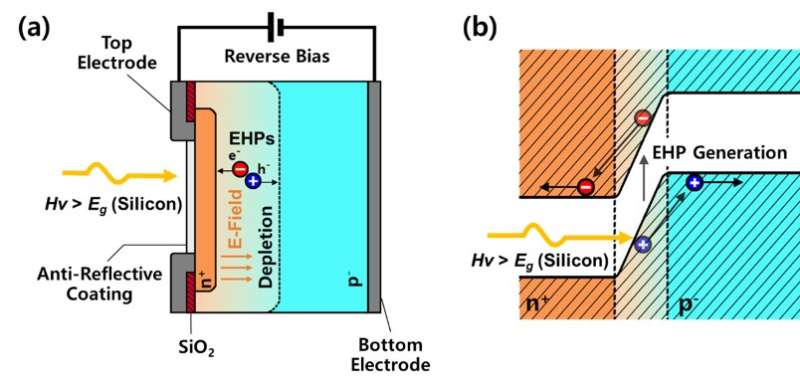
"The operation principle of PN junction photodiodes is as follows: electron-hole-pairs (EHP) are generated in the depletion region when a light source with energy larger than the silicon bandgap is incident," Baek explained. "Since EHPs are separated into the top and bottom electrodes by the internal electric field, photocurrent is generated."
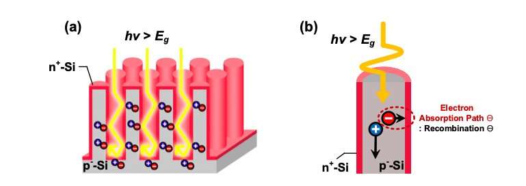
When fabricating the photodiode, the researchers used a radial PN junction that maximizes the light-absorption benefits of a planar PN junction by applying an hourglass-shaped array of SiNWs. The vertical SiNW array in the device has a larger surface area than planar types of arrays. In addition, it can reabsorb primary light from the nanowires surrounding it, which significantly reduces its surface reflectance.

"Since the absorption path of the light source and the electron is separated in the SiNW, the absorption path of the electron can be limited to the diameter of the SiNW. which can reduce the electron recombination when near-infrared having long absorption length is incident perpendicular to the SiNW, thereby generating a large photocurrent," Baek said. "These are the merits of the basic SiNW array and radial PN junction."
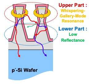
Two further advantages of the hourglass-shaped SiNW arrays devised by the researchers are their resonance and refractive index matching. In fact, the tapered arrangement of the upper inverted-cone-shaped structure enables whispering-gallery-mode resonance. This means that a light source is absorbed by rotating around the surface of the nanowire, thereby enhancing the light absorption path.
"In the lower cone-shaped structure, the smaller the diameter, the more similar to the refractive index of air, so the surface reflectance is much lower than that of bulk silicon. Therefore, it can effectively absorb the reflected or transmitted light source from its upper part," Baek said. "As a result, an hourglass-shaped SiNW photodiode can effectively absorb near-infrared owing to their low surface reflectance and long-effective light absorption length."

The hourglass-shaped SiNW photodiode developed by the Baek and his colleagues enables better absorption of near-infrared light, which has so far proved very difficult for silicon photodiodes with a more conventional shape to absorb. Near-infrared sensing technology can have a variety of applications, for instance, in self-driving LiDAR tech, medical equipment, defense tools, and time-of-flight (TOF) sensors.
"All hourglass-shaped SiNW photodiodes can be fabricated using existing silicon top-down processes, which enables low-cost mass production and high performance reproducibility," Baek said. "In other words, this technology is of great value for its commercialization potential."
In the future, the hour-glass shaped silicon photodiode could enable the development of near-infrared sensing devices for several purposes. In their study, for instance, the researchers used the photodiode to create a heart-rate measurement system that achieved a performance comparable to that achieved by commercially available tools.

"Basic scientific research is important, of course, but as an engineer, I think the most important thing is to do research that can help people in real life," Baek said. "Currently, we are planning two research projects based on our photodiode development experience."
Over the next few months, Baek and his colleagues hope to use the photodiode they developed to create a low-cost and compact TOF sensor, a type of sensing device that is widely used in self-driving vehicles. In addition, they plan to start working with electronics engineering companies to improve the sensitivity of CMOS image sensors (CIS) modules, which are used to fabricate numerous electronic devices, including smartphones.
"A recent study found that the CIS module with improved near-infrared detection yields better images," Baek said. "With same context, we believe that our photodiode development know-how can help improve the near-infrared detection of the CIS modules, thus improving the quality of the acquired image or video."
More information: Kihyun Kim et al. Whispering gallery modes enhance the near-infrared photoresponse of hourglass-shaped silicon nanowire photodiodes, Nature Electronics (2019). DOI: 10.1038/s41928-019-0317-z
© 2019 Science X Network


