AI enhancement for printed circuit boards

Without printed circuit boards (PCBs), there would never have been an electronics revolution. A PCB is the platform upon which minuscule electronic components interact with one another. Today, PCBs are found in an ever-greater number of increasingly complex applications. This has led to increasingly stringent requirements with regard to design and quality assurance. It is vital, for example, to avoid any electrical interference and ensure electromagnetic compatibility. The Fraunhofer Institute for Applied Information Technology FIT has developed a modular AI platform to optimize the design and testing of PCBs, thereby reducing the requisite outlay by as much as 20 percent.
When designing a PCB for a new application, care is taken to make best possible use of the available space and to position components as closely together as possible without risking a failure. At present, this process relies largely on the experience of engineers, whose designs must then be tested in real trials. A further complication is that results are not stringently documented, meaning that error-prone designs undergo repeat testing, which leads to increased costs.
High outlay for quality assurance
Given their complex design, PCBs must be manufactured to extremely exacting specifications. For this reason, each completed PCB undergoes, at the very least, automated optical inspection (AOI). This uses image analysis techniques to determine that the PCB has been produced as per design and therefore does not have any technical defects. At present, however, this method generates a high false negative rate, i.e., a lot of fully functional PCBs are incorrectly classified as defective.
These supposedly defective PCBs must then be inspected once again by hand, either visually or by means of measuring equipment. In other words, an unacceptably high false negative rate means that non-defective PCBs are being rejected and then require reinspection, which in turn results in higher costs. On the other hand, if this rate is too low, the follow-up costs are high as a result of defective components entering the supply chain. It is difficult to achieve an ideal true positive/false negative rate based on human inspection, since human errors also enter into the equation.
Optimal selection based on self-learning techniques
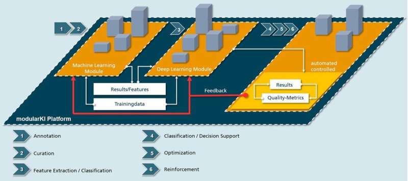
Fraunhofer FIT now shows what a future inspection process can look like. As in conventional automated optical inspection (AOI), a camera records images of the PCB. This improves the quality of the decisions made by the algorithms. Here, it is vital that the modules are provided with high-quality training data. Initially, the modules for machine learning and deep learning are fed with a good selection of data.
"The modular design means we can harness several algorithms, which continually enhance their own performance. Data generated by ongoing automated inspection of components flows back to the algorithm. This then provides the basis for a process of self-learning by the artificial intelligence module," explains Timo Brune, project manager at Fraunhofer FIT. "This permanent feedback enhances the database and optimizes the true negative rate. Early estimates from industry indicate this could reduce the use of production resources by around 20 percent."
Users can train the modules themselves, on the basis of their own process and production data. This means that companies retain control of their own data and are not required to send it to an external server, for example. This toolkit of algorithms can be combined at will for application to specific problems.
Intelligent design of new components
Once trained, the algorithms can also be used to design new PCBs. This ends the lengthy and costly procedure of trial and error whereby components are arranged on the board until the optimal configuration is found. Instead, an algorithm helps to predict which configuration, from a host of options, offers the best functionality.
The PCB application is merely one instance of where a modular, self-enhancing algorithm platform can enhance design and quality assurance. In fact, this approach from Fraunhofer FIT can be applied to many other electrical systems. Here, too, processes can be optimized in order to achieve significant savings in time and production costs.


