October 23, 2020 report
A cleaning-healing-cleaning method to eliminate ionic defects on the surface of perovskite films

A team of researchers affiliated with institutions in the U.K., China and Australia has developed a cleaning-healing-cleaning method that eliminates ionic defects on the surface of 3-D perovskite films. In their paper published in the journal Nature Electronics, the group describes their process and how well it works. Huihui Zhu, Ao Liu and Yong-Young Noh with the University of Science and Technology in Korea have published a News & Views piece in the same journal issue outlining the uses for metal halide perovskite semiconductors, factors limiting their use as field-effect transistors, and the work done by the team on this new effort.
Metal halide perovskite semiconductors have been a subject of research for scientists looking into new ways to build optoelectronic devices. But as Zhu, Liu and Noh point out, the same can not be said for their use in field-effect transistors. This, they explain, is because they suffer from several issues, one of which is ion migration due to screening of applied gate fields by mobile ions in a given channel. The result is reduced current modulation and hysteresis between current and voltage. In this new effort, the researchers developed a method for treating the semiconductors to prevent such problems.
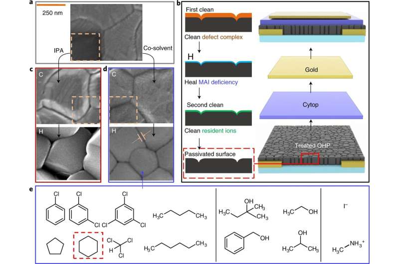
The process they developed is carried out in three steps. The first involves applying a cleaning agent to clear species from the surface that are defective or that have weak bonds. The second step is a healing process that allows for removal of defects or vacancies that result from the first step. The third step involves applying another cleaning agent to clear out ions left behind after the second step. It also makes sure that the surface is entirely clean and that the semiconductor is ready for use.
The researchers note that the cleaning agents were carefully chosen to ensure they did what was required and nothing else. To that end, they chose both polar and non-polar solvents that could be used together in ways that would not alter the structure of the perovskite and would not leave anything behind. They also conducted testing to discover the optimal environmental conditions. The group notes that their work is just one step toward the development of field-effect transistors based on metal halide perovskite semiconductors.
More information: Xiao-Jian She et al. A solvent-based surface cleaning and passivation technique for suppressing ionic defects in high-mobility perovskite field-effect transistors, Nature Electronics (2020). DOI: 10.1038/s41928-020-00486-5
Huihui Zhu et al. Perovskite transistors clean up their act, Nature Electronics (2020). DOI: 10.1038/s41928-020-00470-z
© 2020 Science X Network


