World's first MRAM-based in-memory computing

Samsung Electronics today announced its demonstration of the world's first in-memory computing based on MRAM (Magnetoresistive Random Access Memory). The paper on this innovation was published online by Nature on January 12 (GMT), and is set to be published in the upcoming print edition of Nature. Titled "A crossbar array of magnetoresistive memory devices for in-memory computing," this paper showcases Samsung's leadership in memory technology and its effort to merge memory and system semiconductors for next-generation artificial intelligence (AI) chips.
The research was led by Samsung Advanced Institute of Technology (SAIT) in close collaboration with Samsung Electronics Foundry Business and Semiconductor R&D Center. The first author of the paper, Dr. Seungchul Jung, Staff Researcher at SAIT, and the co-corresponding authors Dr. Donhee Ham, Fellow of SAIT and Professor of Harvard University and Dr. Sang Joon Kim, Vice President of Technology at SAIT, spearheaded the research.
In the standard computer architecture, data is stored in memory chips and data computing is executed in separate processor chips.
In contrast, in-memory computing is a new computing paradigm that seeks to perform both data storage and data computing in a memory network. Since this scheme can process a large amount of data stored within the memory network itself without having to move the data, and also because the data processing in the memory network is executed in a highly parallel manner, power consumption is substantially reduced. In-memory computing has thus emerged as one of the promising technologies to realize next-generation low-power AI semiconductor chips.
For this reason, research on in-memory computing has been intensely pursued worldwide. Non-volatile memories, in particular RRAM (Resistive Random Access Memory) and PRAM (Phase-change Random Access Memory), have been actively used for demonstrating in-memory computing. By contrast, it has so far been difficult to use MRAM—another type of non-volatile memory—for in-memory computing despite MRAM's merits such as operation speed, endurance and large-scale production. This difficulty stems from the low resistance of MRAM, due to which MRAM cannot enjoy the power reduction advantage when used in the standard in-memory computing architecture.
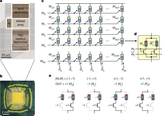
The Samsung Electronics researchers have provided a solution to this issue by an architectural innovation. Concretely, they succeeded in developing an MRAM array chip that demonstrates in-memory computing, by replacing the standard, 'current-sum' in-memory computing architecture with a new, 'resistance sum' in-memory computing architecture, which addresses the problem of small resistances of individual MRAM devices.
Samsung's research team subsequently tested the performance of this MRAM in-memory computing chip by running it to perform AI computing. The chip achieved an accuracy of 98% in classification of hand-written digits and a 93% accuracy in detecting faces from scenes.
By ushering MRAM—the memory which has already reached commercial-scale production embedded in the system semiconductor fabrication—into the realm of in-memory computing, this work expands the frontier of the next-generation low-power AI chip technologies.
The researchers have also suggested that not only can this new MRAM chip be used for in-memory computing, but it also can serve as a platform to download biological neuronal networks. This is along the line of the neuromorphic electronics vision that Samsung's researchers recently put forward in a perspective paper published in the September 2021 issue of the journal Nature Electronics.
"In-memory computing draws similarity to the brain in the sense that in the brain, computing also occurs within the network of biological memories, or synapses, the points where neurons touch one another," said Dr. Seungchul Jung, the first author of the paper. "In fact, while the computing performed by our MRAM network for now has a different purpose from the computing performed by the brain, such solid-state memory network may in the future be used as a platform to mimic the brain by modeling the brain's synapse connectivity."
As highlighted in this work, by building on its leading memory technology and merging it with system semiconductor technology, Samsung plans to continue to expand its leadership in next-generation computing and AI semiconductors.
More information: Seungchul Jung et al, A crossbar array of magnetoresistive memory devices for in-memory computing, Nature (2022). DOI: 10.1038/s41586-021-04196-6


