November 26, 2022 report
Building a 900-pixel imaging sensor using an atomically thin material

A team of researchers at Penn State University has developed a 900-pixel imaging sensor using an atomically thin material. In their paper published in the journal Nature Materials, the group describes how they built their new sensor and possible uses for it.
Sensors that react to light have become very common in the modern world—lights that turn on when the presence of an intruder is detected, for example. Such sensors are typically made of a grid of pixels, each of which are reactive to light. Performance of such sensors are based on measurements of responsivity, and which parts of light they detect.
Most are designed with certain noise-to-signal constraints. In this new effort, the researchers noted that most such sensors are also very inefficient, using far more electricity than should be the case for such devices.
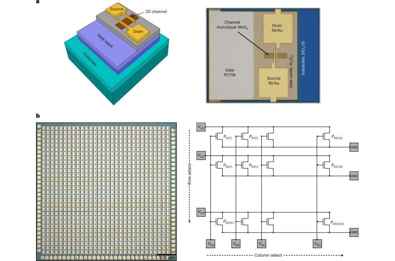
To make a sensor that would be more efficient, the researchers looked at the materials that are used to make those now in use—generally a silicon complementary metal oxide semiconductor serves as the backbone. And it was the backbone where the researchers focused their effort. To make a sensor that would be more efficient, they replaced the traditional backbone with one made from molybdenum disulfide, a material that, like graphene, can be grown as a one atom thick sheet.
In their work, they grew it on a sapphire base via vapor deposition. Then then lifted the finished product from the base and laid it on a base of silicon dioxide that had already been wire etched. They then finished their product by etching additional wiring on the top.
The result of their work was a 30x30 grid, where each of the pixels was its own device—one that was not only capable of detecting light but could also be drained using an electrode that made it ready for use again after something has been sensed.
In assessing the characteristics of their sensor, they found it to be far more efficient than those now in use, each pixel used less than a picojoule. They also found it very easy to reset. One shot of voltage across the array did the trick. On the other hand, the researchers found that it responded far slower to light than sensors currently in use. This, they note, suggests it could be used as an all-purpose light sensor, but not as fixture in a camera. They further suggest it could provide an ideal sensing solution in a wide variety of IoT applications.
More information: Akhil Dodda et al, Active pixel sensor matrix based on monolayer MoS2 phototransistor array, Nature Materials (2022). DOI: 10.1038/s41563-022-01398-9
© 2022 Science X Network


