This article has been reviewed according to Science X's editorial process and policies. Editors have highlighted the following attributes while ensuring the content's credibility:
fact-checked
peer-reviewed publication
trusted source
proofread
World's first mass production of metalenses for visible wavelengths

Do you hate the camera bumps on the back of your smartphone? A new optical component called metalens—which was named one of the top 10 future technologies by the World Economic Forum in 2019—may be the answer. Composed of a nanostructured array, this incredibly thin and lightweight optical device is currently the focus of much attention in the scientific community, even featured in a special issue of Nature Photonics. However, the production of metalenses requires highly precise techniques and can be expensive, posing a challenge for their scalable manufacturing.
In a groundbreaking achievement, a team of researchers from POSTECH led by Professor Junsuk Rho (Department of Mechanical Engineering, Department of Chemical Engineering) has successfully mass-produced metalenses for visible light, the first in the world to do so. The team also included Ph.D. candidates Joohoon Kim and Junhwa Seong, (Department of Mechanical Engineering at POSTECH), as well as Professor Heon Lee and Wonjoong Kim from the Department of Materials Science and Engineering at Korea University, and Dr. Gyoseon Jeon and Dr. Dong Hyun Yoon from the Research Institute of Industrial Science and Technology (RIST). The findings from their study were recently published in Nature Materials.
The team overcame the limitations of the fabrication process by combining two techniques used in semiconductor and display manufacturing: Photolithography uses light to pattern a substrate, similar to taking a photography, while nanoimprint lithography involves using a stamp with nano-sized patterns to print patterns onto a substrate.
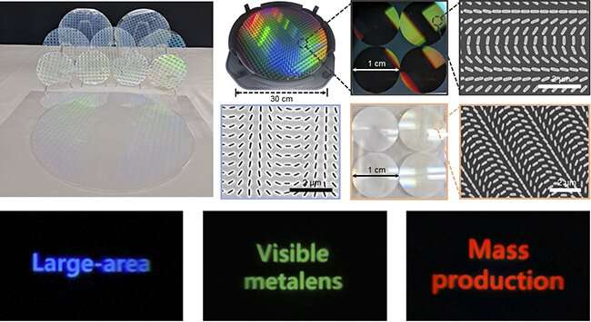
The researchers first created a single pattern using electron beam lithography, then replicated the pattern using deep-ultraviolet ArF photolithography to create 12-inch master stamp. Using the stamp and nanoimprint lithography, they were able to successfully produce metalenses with a 1 cm diameter at a high speed.
Conventional nanoscale structures based on nanoimprint technology had low refractive indices, resulting in very low efficiencies of around 10%, requiring significant costs to improve their efficiency. The research team succeeded in improving the efficiency of the lens up to 90% by coating the lens with a very thin layer of titanium dioxide (TiO2) of about 20 nanometers. By combining the two technologies, the team was able to mass-produce high-performance metalenses with a simple process.
The team also demonstrated the practicality of metalenses by creating lightweight virtual reality (VR) devices capable of displaying images in red, green, and blue. The study takes a step closer to commercializing metalenses through the synergy of the two existing technologies and has been selected as the inaugural project of the POSCO-POSTECH-RIST Convergence Research Institute. The success of the mass production of metalenses is anticipated to accelerate their commercialization and provide a significant opportunity for POSCO's transformation from a steel manufacturer to a future-oriented material company.
In response to the success of the research, Professor Junsuk Rho, the lead researcher, shared his thoughts on the achievement: "This study demonstrates the possibility of taking meta-material research, which has been in the research stage for 20 years without commercialization, to the industrial stage and making it applicable in real life. The significance of this achievement lies in the fact that we have succeeded in mass-producing metalenses for visible light on a wafer scale, which is the most advanced technology in the world."
More information: Joohoon Kim et al, Scalable manufacturing of high-index atomic layer–polymer hybrid metasurfaces for metaphotonics in the visible, Nature Materials (2023). DOI: 10.1038/s41563-023-01485-5


