July 31, 2024 feature
This article has been reviewed according to Science X's editorial process and policies. Editors have highlighted the following attributes while ensuring the content's credibility:
fact-checked
peer-reviewed publication
trusted source
proofread
A strategy to synthesize fin-like metal nanosheets for 2D transistors

The effective integration of extremely thin insulating layers with two-dimensional (2D) semiconductors could enable the fabrication of 2D transistors with an electrical capacitance comparable to SiO2 with thicknesses below 1-nm. These transistors could, in turn, help to boost the performance and reduce the power consumption of electronic devices.
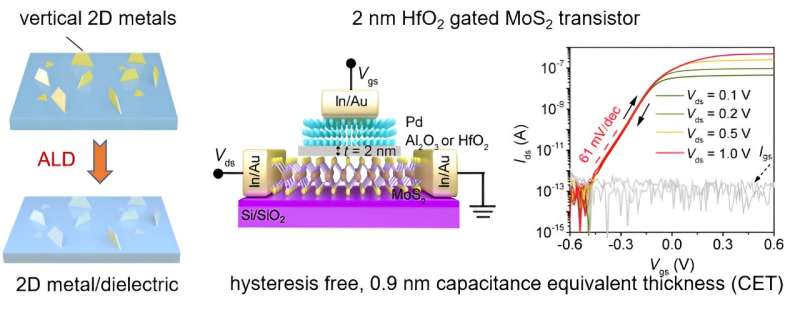
Researchers at Nankai University in China recently introduced a new strategy to synthesize single-crystalline metal nanosheets that could be easily transferred onto 2D substrates. This strategy, outlined in a paper in Nature Electronics, was successfully used to deposit 2-nm-thick dielectrics based on Al2O3 or HfO2 for highly performing top-gated transistors.
"At the very beginning, we aimed to developing the chemical vapor deposition (CVD) synthetic strategy of 2D Cu2O, which is a p-type high-mobility 2D semiconductor," Jinxiong Wu, corresponding author of the paper, told Tech Xplore.
"However, we got the elementary Cu metal instead by using the CuCl and Bi2O3 as the reaction precursors. Moreover, by changing the types of metal chlorides, we can also get other 2D metals, such as Pd and Au."
When reviewing previous literature, Wu and his colleagues found that 2D metals based on Pd and Au had not yet been synthesized using CVD, which is a process commonly used to produce thin films or materials on a substrate. Interestingly, they also realized that almost all 2D metal nanosheets have atomically flat surfaces and could be vertically grown on a substrate.
"I have been always asking myself and my students 'what can we do with this knowledge?'," Wu said. "Just when we were about to give up the project, the configuration of fin field-effect transistor inspired me.
"If we can integrate the vertically grown 2D metals with atomically thin atomic-layer-deposited (ALD) dielectrics, it can avoid the compatibility problem between ALD technology and 2D semiconductors, and the destructive step of top-gate electrode deposition onto ultrathin dielectrics, offering a route to fabricating 2D FETs with sub-nanometer capacitance equivalent thickness."
To integrate metal nanosheets and dielectric materials, Wu and his students directly deposited atomically thin and flat dielectrics, namely Al2O3 and HfO2, on vertically grown 2D metals. Unlike the 2D transition metal sulfide molybdenum disulfide (MoS2), which is commonly used as a channel semiconductor in transistors, 2D metals have a surface compatible with ALD techniques. After the ALD growth, the metal/oxide stack can be integrated with 2D semiconductors using a one-step process that forms a van der Waals interface.
The recent study by this team of researchers introduced a highly promising approach to fabricate 2D transistors based on 2D metals and atomic-layer-deposited dielectrics. Their proposed strategy entails the use of ultra-smooth vertical 2D metals to enable the high-quality ALD growth of ultrathin high-κ oxides, as well as the subsequent one-step van der Waal integration of metal/oxide stacks.
"Our strategy does not only address the incompatibility problem between ALD technology and 2D semiconductor, but can also avoid the destructive step of top-gate electrode deposition process onto the ultrathin dielectrics, thus making the big challenge of scaling the CET value of seed-layer-free 2D FETs to sub-nanometer possible," Wu said.
As part of their study, the researchers used their proposed CVD strategy to create 2-nm-thick dielectrics based on Al2O3 or HfO2, which they then used to fabricate top-gated transistors. In initial tests, the resulting transistors attained promising results, exhibiting leakage currents of 10−6 A cm−2, low operating voltages of around 0.45 V and a hysteresis below 1 mV.
"We believe the developed methodology of Bi2O3-assisted CVD growth is an important advancement in the field of CVD growth of 2D materials, as it enables the synthesis of some new 2D materials that are difficult to synthesize using traditional methods," Wu added. "We are now planning to achieve wafer-scale fabrication of hysteresis-free 2D transistors with capacitance equivalent thickness below 1 nm."
More information: Lei Zhang et al, Vertically grown metal nanosheets integrated with atomic-layer-deposited dielectrics for transistors with subnanometre capacitance-equivalent thicknesses, Nature Electronics (2024). DOI: 10.1038/s41928-024-01202-3.
© 2024 Science X Network


