Amorphous boron nitride shows excellent insulating properties for next generation of electronics

In the ongoing process of miniaturization of logic and memory devices in electronic circuits, reducing the dimensions of interconnects—metal wires that link different components on a chip—is crucial to guarantee fast response of the device and improve its performance. Research efforts have been focused on developing materials with excellent insulating properties to separate the interconnects from each other. A suitable material for this application is required to have a dielectric constant (parameter that defines its insulating properties) no higher than 2. Furthermore, it should serve as a diffusion barrier against migration of metals into semiconductors and be thermally, chemically and mechanically stable.
The quest for such a heavily insulating material has driven the semiconductor industry for at least the past 20 years. However, while over time materials with the desirable characteristics above have been reported (organic polymeric materials and others) and have created excitement in the industry, they have systematically failed to be successfully integrated in interconnects due to poor mechanical properties or insufficient chemical stability upon integration, causing reliability failures.
In a paper published today in Nature, researchers have achieved the first large-scale synthesis of thin film of amorphous Boron Nitride (a-BN) showing record low dielectric characteristics. This is a groundbreaking achievement which suggests that a-BN is an excellent candidate for application in high-performance electronics. The first author of the article is Seokmo Hong and another is Prof. Hyeon Suk Shin, both from the Department of Chemistry of Ulsan National Institute of Science and Technology.
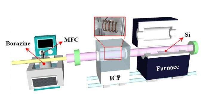
In particular, a-BN as thin as 3nm was synthesized on a silicon substrate (using low temperature inductively coupled plasma-chemical vapor deposition, ICP-CVD), which showed an exceptionally low dielectric constant of 1.78 at 100 kHz. Tests of the diffusion barrier properties of this amorphous material, conducted in very harsh conditions, have also demonstrated that it is able to prevent metal atom migration from the interconnects into the insulator. Together with a high breakdown voltage, these characteristics makes a-BN very attractive for practical electronic applications.
State-of-the-art techniques, such as HRTEM, XPS, Raman spectroscopy, FTIR, PEY-NEXAFS, have been successfully employed to characterize the material. In contrast to other materials with a low dielectric constant, which are sometimes made porous to exploit the low dielectric constant of air at the expense of mechanical strength, a-BN film features the lowest dielectric constant at the highest density. Remarkably, measurements also indicate that the material has hardness and stiffness larger than bulk silicon.

To explain the correlation between the structural and morphological properties and the dielectric response of the a-BN film, Dr. Aleandro Antidormi from the ICN2 Theoretical and Computational Nanoscience Group, led by ICREA Prof. Stephan Roche, has performed atomistic calculations on samples of a-BN generated "in silico." By means of classical molecular dynamics, the chemical vapor deposition (CVD) method employed experimentally was simulated to build an a-BN film on Si having similar dimensions as the fabricated one. Ultimately, the calculations helped identifying the key factors for the excellent performances of a-BN: the nonpolar character of the BN bonds and the lack of order preventing dipoles alignment. The results of this simulation have contributed to understanding the structural morphology of this amorphous material as well as to explaining its superior dielectric performances.
More information: Seokmo Hong et al. Ultralow-dielectric-constant amorphous boron nitride, Nature (2020). DOI: 10.1038/s41586-020-2375-9


