Team develops technique for printing circuits on irregular surfaces with pulses of light

Printable electronics could cause a proliferation of smart, connected devices, from household appliances that can communicate with each other to medical diagnostic sensors that can be placed on the body to forgo invasive procedures. But the variety of printing surfaces poses a challenge, since a method used to print on a flat object may not be safe for use on human skin or applicable for complicated textures and shapes.
Led by Penn State, an international team of researchers has developed a low-cost, low-heat transfer technique that can print biodegradable electronics on a variety of complex geometries and, potentially, human skin. They published their findings today in Materials Today.
"We are trying to enable direct fabrication of circuits on freeform, 3D geometries," said Huanyu "Larry" Cheng, Dorothy Quiggle Career Development Professor in Penn State's Department of Engineering Science and Mechanics (ESM). "Printing on complicated objects can allow a future Internet of Things where circuits can connect various objects around us, whether they be smart home sensors, robots performing complex tasks together, or devices placed on the human body."
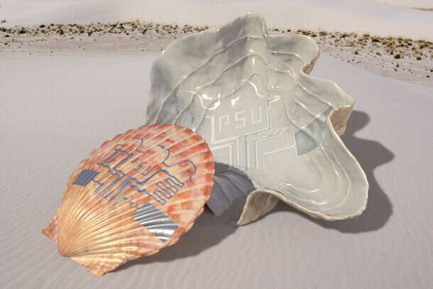
To begin the printing process, researchers covered a thin film with an ink made from zinc nanoparticles. This thin film was attached to a stencil-like overlay on the target surface. The researchers then pulsed a high-energy xenon light through the film. Within milliseconds, energy from this light excited the particles enough to transfer them to the new surface through the stencil. And that new surface, with this method, could be complex in shape: Printed objects in the experiment included a glass beaker and a seashell. The transferred zinc formed a conductive electronic circuit that could be adapted for use as a sensor or antenna.
The method, compared to other electronics printing techniques, is much faster and cost-efficient because it does not use expensive equipment like vacuum chambers that require hours of operation to reach the appropriate pressure, Cheng said. It can also be more sustainable.
"Our electronics upgrade every two years or so, and this creates a huge amount of electronic waste," Cheng said. "When we look at the future, if our electronics are green enough to be flushed down the toilet, their use will be much better for the environment."
This biodegradability factor also improves the security of such devices. Conventional silicon-based electronics can be secured with encryption software, but a biodegradable electronic takes security one step further.
"If your device is only encrypted with software, it can always be cracked and there's a potential leak for information," said Cheng. "This biodegradable device can be physically destroyed so that data can't be recovered; it presents a unique opportunity that can't be addressed by traditional silicon devices."
The team also explored options to convert the printed biodegradable zinc circuits into permanent circuits. The researchers submerged the printed surfaces into solutions containing copper or silver. Through a chemical replacement process, the zinc-based circuits became either silver-based or copper-based, allowing for longer-term use of the circuit.
In the future, the team plans to investigate ways to make the printing process more friendly to large-scale manufacturing. Optimization of the printing procedure, as well as printing on skin for health monitoring applications, will also be a priority.
Other contributors to this study include Ning Yi, affiliated with the Penn State Department of Materials Science and Engineering; Yuyan Gao, Antonino Lo Verso Jr., Daniel Erdely and Jia Zhu with ESM; Cuili Xue with Shanghai Jiao Tong University; and Robert Lavelle with the Applied Research Laboratory at Penn State.
More information: Ning Yi et al, Fabricating functional circuits on 3D freeform surfaces via intense pulsed light-induced zinc mass transfer, Materials Today (2021). DOI: 10.1016/j.mattod.2021.07.002


